Out With Organic, In With Glass? DNP Unveils Glass Core Substrate Tech For Chips
by Anton Shilov on March 23, 2023 11:00 AM EST- Posted in
- Semiconductors
- Packaging
- DNP
- Dai Nippon Printing
As the chip industry develops more sophisticated processors with higher heat dissipation requirements, some firms have moved on to chiplet-based designs. This not-so-gradual shift has resulted in chip packaging technologies becoming increasingly important. Large and highly complex chips such as Nvidia's H100 and advanced multi-chip solutions like Intel's Data Center Max GPU (Ponte Vecchio) present new requirements for packaging materials. To that end, Dai Nippon Printing (DNP) is showcasing a new development for semiconductor packages – Glass Core Substrate (GCS) – which it says can address many of those challenges.
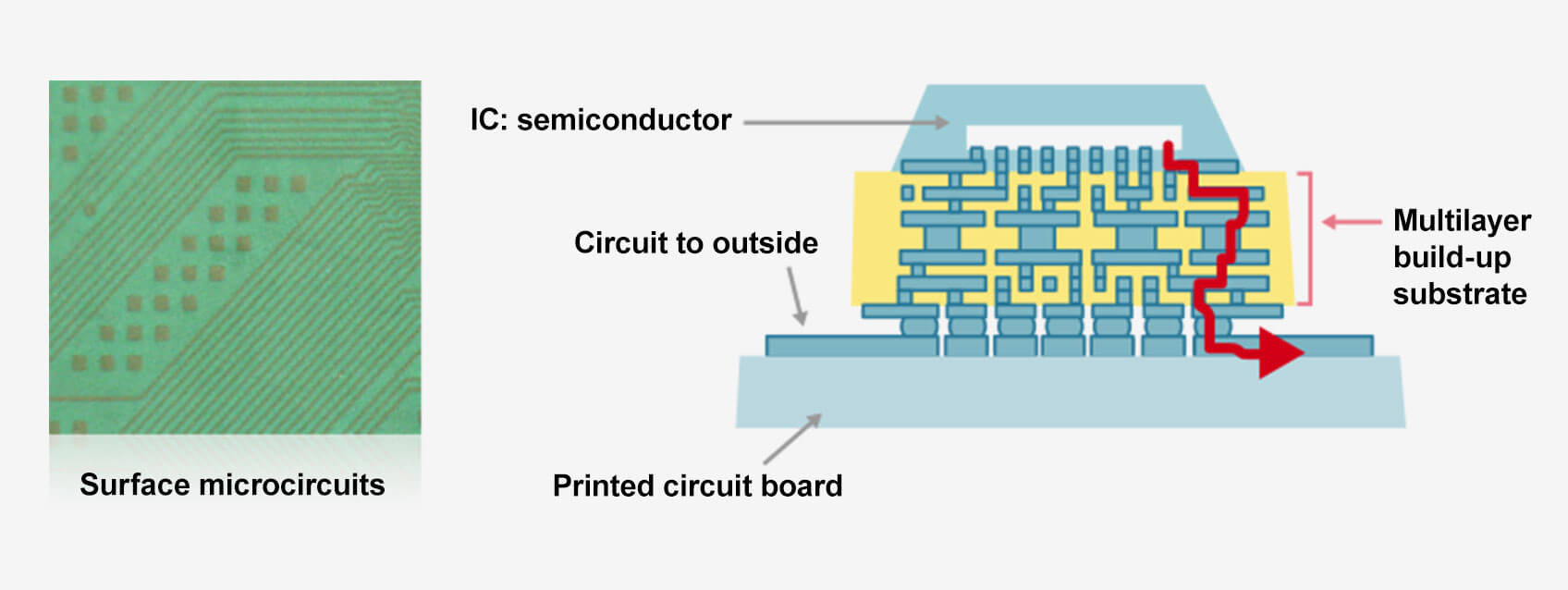
Typically, modern chips are installed on fine pitch substrates (FPS), which are then put on multi-layer high-density interconnect (HDI) substrates. The most advanced CPU/GPU HDI substrates these days use Ajinomoto Build-up Film(ABF), which combines organic epoxy resins, hardener, and inorganic microparticle filler, according to the manufacturer. It is easy to use, and it can achieve high-density pitching (thus enabling high density metal wiring), it has insulation properties that are good enough for modern chips, high rigidity, high durability, and low thermal expansion, among other factors.
Will ABF and other organic resin-based substrates still be good enough for chiplets? Well, it's quite a challenge, as these multi-chiplet designs will be more power-hungry (and thus hotter) and require metal writing of a higher density due to the widening of memory and I/O interfaces. This increase in power requirements puts added pressure on the outlying substructure of the circuitry. Finding new materials to use within the core makeup of chips within the semiconductor industry has been a hot pursuit for many years.
One such company in the semiconductor industry is Dai Nippon Printing (DNP), and they claim that their HDI substrates with a glass core have superior properties compared to organic resin-based substrates. According to Dai Nippon, using a glass core substrate (GCS) can enable finer pitching and, therefore, extremely dense wiring because it is stiffer and less prone to expansion due to high temperatures. A schematic drawing demonstrated by DNP even omits the fine pitch substrate from the packaging altogether, implying that this part may no longer be needed.

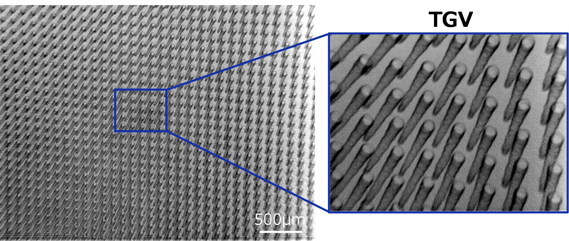
Perhaps, most notably, DNP claims its glass core substrate can offer high through glass via (TGV) density (compatible with FPS) with a high aspect ratio. The aspect ratio, in this case, is the ratio between the thickness of the glass and the diameter of the via. As the number of vias increases and the ratio increases, the processing of substrates gets harder, and maintaining the rigidity gets more challenging.
Glass is considered more rigid than organic resin-based substrates and has several advantages, but the adhesion between glass and copper (or other metal wires) is still a major challenge in regard to bonding. The DNP-developed glass substrate has an aspect ratio of 9 and ensures adhesiveness to enable fine pitch-compatible wiring. Since there are only a few GCS thickness constraints, there is a lot of freedom when it comes to maintaining a balance between thickness, warpage, stiffness, and smoothness, the company says.
Dai Nippon Printing produces out-coupling enhancement structures for LCDs and scattering for backlighting modules, so it has vast experience with the mass production of glass-based structures. Meanwhile, DNP is not the only specialist in rigid glass applications looking ahead to the future in making HDI substrates for advanced chips or multi-chiplet solutions. Corning has been exploring this area for quite a while, though it does not look like its technology is used commercially for high-volume chips or in multi-chip-modules.
Source: Dai Nippon Printing


17 Comments
View All Comments
name99 - Thursday, March 23, 2023 - link
The A16 has a very strange packaging (vaguely described in this article).https://eetimes.itmedia.co.jp/ee/articles/2210/25/...
It *seems* to be something like the above, with a glass slab, DRAM on one side, and TGVs connecting to the SoC on the other side.
It's certainly very different from the standard PoP as used by iPhones (and other phones) since forever.
Everything about this packaging is mysterious, but one wonders if it was something of a trial run for future M-series designs that put the DRAM "behind" rather than "beside" the SoC. For that to work you need a large enough substrate to reach to Ultra (or the mythical Extreme) sizes, but if DNP can do this at ~5cm x 5cm maybe that's large enough.
For your extra cost presumably you get improved electrical stiffness (ie lower capacitance, and so higher frequency signals and/or lower energy wasted in the DRAM<->SoC traffic).
The other thing you have to bear in mind with these sorts of designs is thermal expansion. You don't want the substrate to expand at a slightly different rate from the SoC and thus put mechanical strain on the connecting wires... And this becomes more and more of an issue as you grow larger.
Presumably the glass has been matched to silicon's coefficient of thermal expansion, and this may be a lot easier to achieve (and thus worth it just for that functionality) than trying to match a resin substrate to Si thermal expansion? The other alternative of course is to use Si itself as the substrate, but that's another leap in expense, so if glass can replace many of those Si interposer use cases...
The article calls the A16 slab "glass epoxy" as opposed to just "glass" but who knows what that means?
Wereweeb - Thursday, March 23, 2023 - link
"Glass epoxy" is fibreglass, i.e. organic substrate. Nothing strange about it.Samus - Friday, March 24, 2023 - link
How is glass epoxy 'organic' when epoxy is a thermoplastic polymer, a synthetic material?AdrianBc - Friday, March 24, 2023 - link
In chemistry, the most frequently used definition of the term "organic substance" is a chemical substance composed of molecules that include covalent carbon-carbon bonds.The reason is that this kind of chemical substances have been initially discovered by the study of substances extracted from the bodies of living beings, even if nowadays such substances are produced also or only by artificial chemical synthesis.
When the materials used in fabrication processes are described, the standard chemical terminology is used, unlike when advertising food or dietary supplements.
Wereweeb - Friday, March 24, 2023 - link
Ah, yes, now I understand, the fault lays with the "organic food" yank nonsense.Personally I much prefer the inorganic kind of food, like clay cookies and limestone pastries.
LiKenun - Saturday, March 25, 2023 - link
An excellent source of minerals like calcium!mode_13h - Sunday, March 26, 2023 - link
At least they have a longer shelf-life!Wereweeb - Friday, March 24, 2023 - link
Organic = hydrocarbon-based. Petroleum and almost all of it's derivates are organic by definition.I can't fathom how you could possibly be confused about that, since we're talking about primary school level chemistry.
III-V - Friday, March 24, 2023 - link
Most primary schools don't cover chemistry at all, lolThreska - Saturday, March 25, 2023 - link
Is that were we all learned to be the unabomber?