NVIDIA Announces Quadro GP100 - Big Pascal Comes to Workstations
by Ryan Smith on February 5, 2017 6:01 PM EST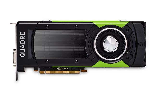
Kicking off on this Sunday afternoon is CAD & CAE software developer Dassault Systèmes’ annual trade show, the aptly named SOLIDWORKS World. One of the major yearly gatherings for workstation hardware and software vendors, it’s often used as a backdrop for announcing new products. And this year NVIDIA is doing just that with a literal Big Pascal product launch for workstations.
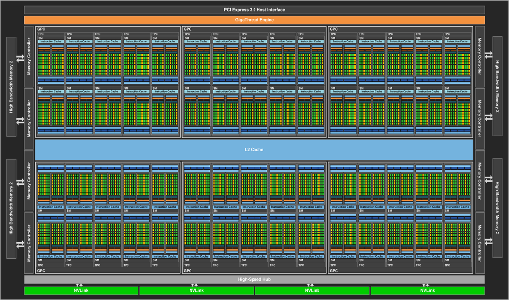
The last time we checked in on NVIDIA’s Quadro workstation video card group, they had just launched the Quadro P6000. Based on a fully enabled version of NVIDIA’s GP102 GPU, the P6000 was the first high-end Quadro card to be released based on the Pascal generation. This is a notable distinction, as NVIDIA’s GPU production strategy has changed since the days of Kepler and Maxwell. No longer does NVIDIA’s biggest GPU pull triple-duty across consumer, workstations, and servers. Instead the server (and broader compute market) is large enough to justify going all-in on a compute-centric GPU. This resulted in Big Pascal coming to life as the unique GP100, while NVIDIA’s graphical workhorse was the smaller and more conventional (but still very powerful) GP102.
Because of this split in NVIDIA GPU designs, it wasn’t clear where this new compute-centric GPU would fit in across NVIDIA’s product lines. It’s the backbone of Tesla server cards, of course, and meanwhile it’s very unlikely to show up in consumer GeForce products. But what about the Quadro market, which in previous generations has catered to both graphics and compute users at the high-end (if only because of the mixed-use nature of previous generation GPUs)? The answer, as it turns out, is that Big Pascal has a place in the Quadro family after all. And that’s an interesting place at the top that NVIDIA calls the Quadro GP100.
Based on NVIDIA’s GP100 GPU, Quadro GP100 defies a simple explanation due in large part to GP100’s unique place in NVIDIA’s Pascal GPU family. Quadro GP100 on one hand a return to form for NVIDIA’s Quadro lineup. It’s the jack of all trades card that does everything – graphics and compute – including features that the Tesla cards don’t offer, a job previously fulfilled by cards like the Quadro K6000. On the other hand, it’s not necessarily NVIDIA’s most powerful workstation card: on paper its FP32/graphics performance is lower than Quadro P6000’s. So where does Quadro GP100 fit in to the big picture?

The long and short of it is that the Quadro GP100 is meant to be a Tesla/GP100 card for workstations, but with even more functionality. While NVIDIA offers PCIe Tesla P100 cards, those cards only feature passive cooling and are designed for servers; the lack of active cooling means you can’t put them in (conventional) workstations. The Quadro GP100 on the other hand is a traditional, fan & shroud active cooled card, like the rest of the Quadro lineup. And then NVIDIA doesn’t stop there, enabling graphics functionality that isn’t on the Tesla cards. The fact that NVIDIA isn’t even giving it a P-series name – rather naming it after the GPU underneath – is a good hint of where NVIDIA is going.
| NVIDIA Quadro Specification Comparison | ||||||
| GP100 | P6000 | M6000 | K6000 | |||
| CUDA Cores | 3584 | 3840 | 3072 | 2880 | ||
| Texture Units | 224 | 240 | 192 | 240 | ||
| ROPs | 128? | 96 | 96 | 48 | ||
| Boost Clock | ~1430MHz | ~1560MHz | ~1140MHz | N/A | ||
| Memory Clock | 1.4 Gbps HBM2 | 9Gbps GDDR5X | 6.6Gbps GDDR5 | 6Gbps GDDR5 | ||
| Memory Bus Width | 4096-bit | 384-bit | 384-bit | 384-bit | ||
| VRAM | 16GB | 24GB | 24GB | 12GB | ||
| ECC | Full | Partial | Partial | Full | ||
| FP64 | 1/2 FP32 | 1/32 FP32 | 1/32 FP32 | 1/3 FP32 | ||
| TDP | 235W | 250W | 250W | 225W | ||
| GPU | GP100 | GP102 | GM200 | GK110 | ||
| Architecture | Pascal | Pascal | Maxwell 2 | Kepler | ||
| Manufacturing Process | TSMC 16nm | TSMC 16nm | TSMC 28nm | TSMC 28nm | ||
| Launch Date | March 2017 | October 2016 | 03/22/2016 | 07/23/2013 | ||
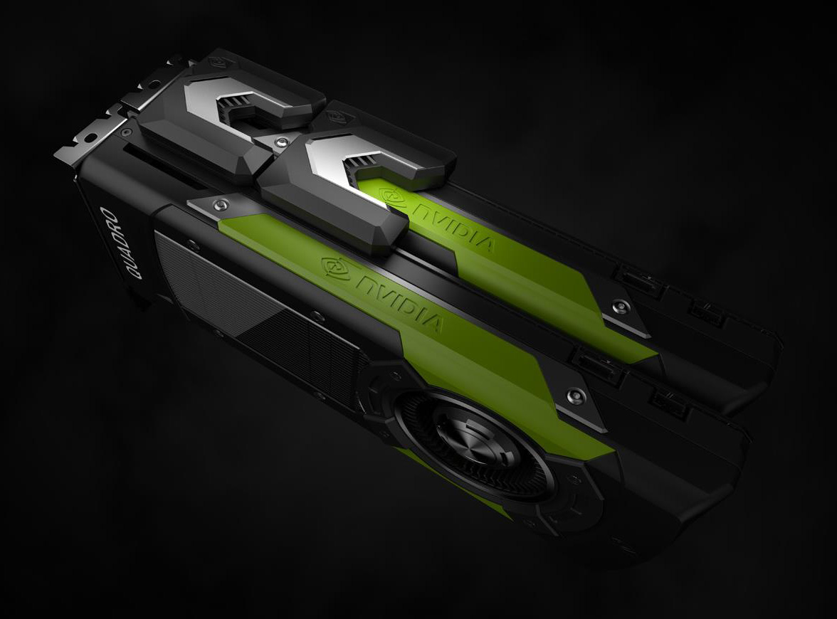
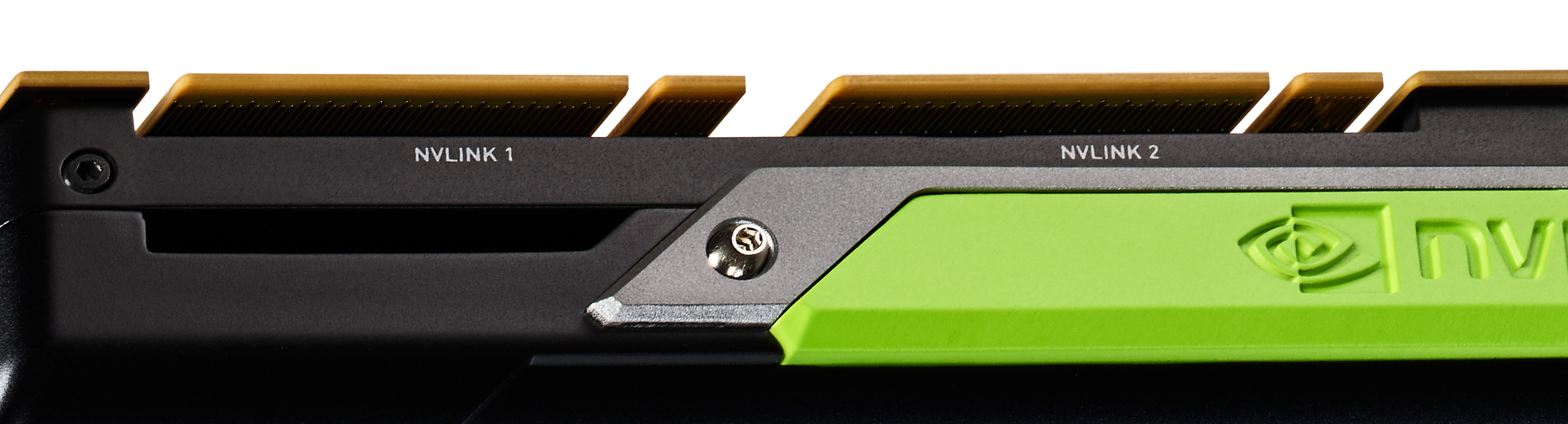
The Quadro GP100 then is being pitched at an interesting mix of users. For compute users who need a workstation-suitable GP100 card, then the Quadro GP100 is meant to be their card. It offers all of GP100’s core functionality, including ECC memory, half-speed FP64, and double-speed (packed) FP16 instructions. As an added kicker, the Quadro GP100 introduces a new NVLink connector for PCIe cards. This allows for a pair of Quadro cards to be linked up in a 2-way NVLink configuration, bringing with it NVLInk’s memory access and low latency data transfer benefits to PCIe cards. Notably, this isn’t available on the Tesla PCIe cards.
As NVIDIA discusses it, they sound rather confident that Quadro GP100 will sell well to compute users, and for good reason. The Tesla P100 cards have been a hit with neural network programmers, and now researchers have a card suitable for dropping into a workstation to develop against.
Meanwhile the second market for the Quadro GP100 is the traditional high-end CAD/CAE market. For those more specialized users who need a workstation card with fast FP64 performance and ECC memory for maximum accuracy and reliability, the Quadro GP100 is the first Quadro card since the K6000 to offer that functionality. Arguably this is a bit of a niche, since most CAD users don’t need that kind of reliability, but for those who do for complex engineering simulations and the like, it’s critical (not to mention a lucrative market for NVIDIA). Serving this market also makes the Quadro GP100 unique in that it’s the only GP100 card with its graphical functionality turned on.
However when it comes to those graphical workloads, this is where the line between the Quadro GP100 and P6000 gets a lot murkier. The Quadro P6000 is rated for 12 TFLOPS FP32, versus GP100’s 10.3 TFLOPS, and similarly the Quadro GP100 features around 86% of the texture throughput as well. Paper specs aren’t everything, of course, but in pure SM throughput-bound scenarios the P6000 should be the faster card. This being the advantage of the more compact (and manufacturable) GP102 versus the massive GP100.
The one wildcard here is the HBM2 memory interface and associated ROPs. NVIDIA is specifically touting the Quadro GP100 as offering their fastest rendering performance, and depending on the scenario that can very well be the case. With 720GB/sec of memory bandwidth – thanks to 4 HBM2 stacks clocked at 1.4Gbps each – the Quadro GP100 has 66% more memory bandwidth than the Quadro P6000’s mere 432GB/sec. Coupled with what’s almost certainly a ROP count advantage – NVIDIA still hasn’t disclosed GP100’s ROP count, but based on what we know of GP102, 128 ROPs is a safe bet – and Quadro GP100’s pure pixel pushing power should be greater than even P6000 by around 22%. Given that CAD/CAE can be very pixel-bound, and this should be a tangible benefit for some Quadro customers.
The one drawback though is memory capacity. While the Quadro P6000 offers 24GB of VRAM due to the greater practical capacity of GDDR5X, like all GP100 products the Quadro GP100 tops out at 16GB of HBM2. This means that for very large dataset users, a single Quadro GP100 is a good deal smaller than what they can get out of the P6000. It’s worth noting that NVIDIA is touting NVLink as helping out with memory crunch issues, however I suspect that’s rooted in compute more than graphics.
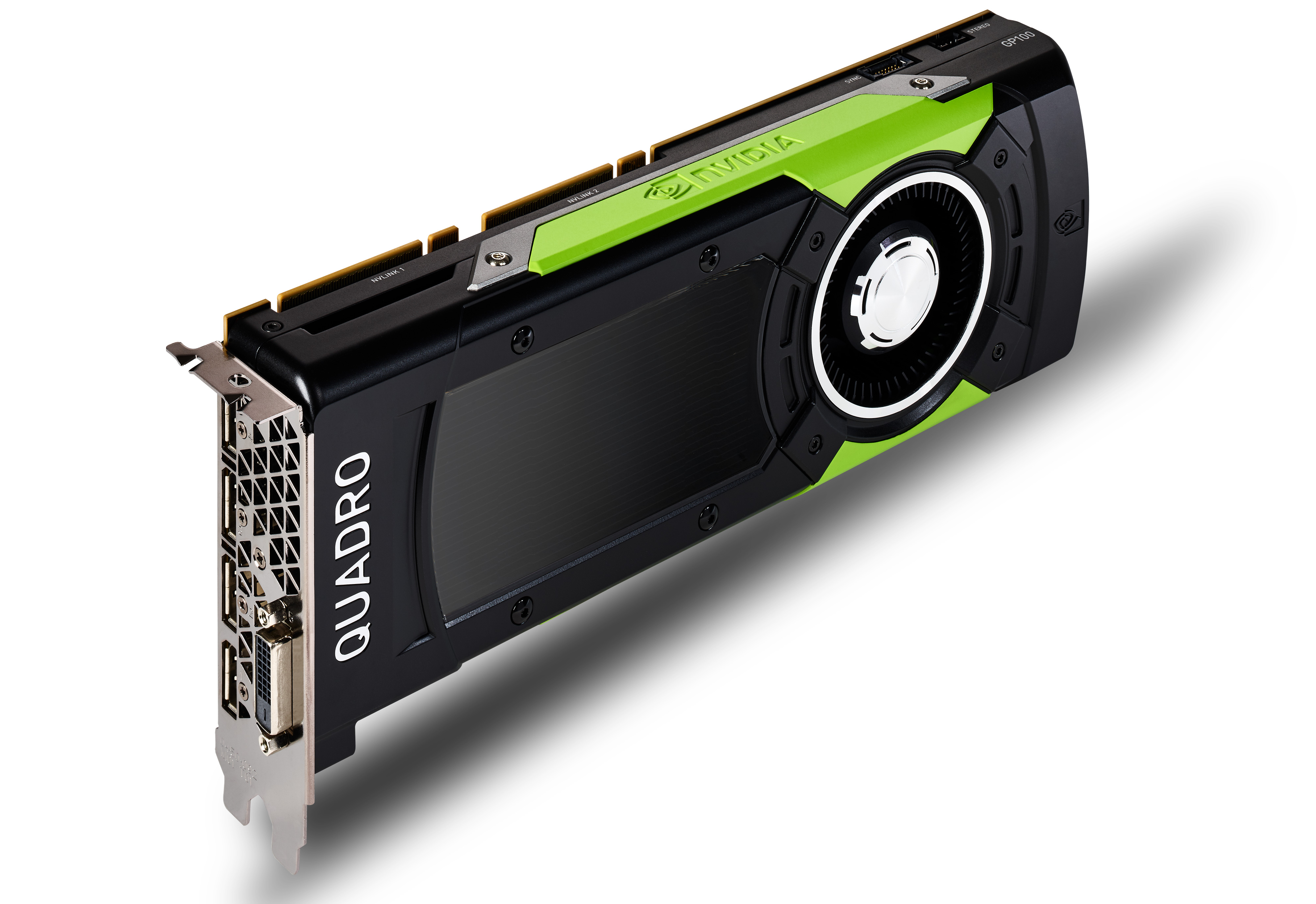
Moving on then, outside of the GPU underneath, the Quadro GP100 packs the typical Quadro family hardware features. This includes 4 DisplayPort 1.4 ports and a single DVI port for display outputs, and NVIDIA is classifying it as VR Ready as well. Meanwhile towards the rear of the card are the Quadro Sync and Stereo connectors for synchronized refresh and quad-buffered stereo respectively.
Wrapping things up, like the rest of the Quadro cards being launched today, NVIDIA is expecting the Quadro GP100 to ship in March. Pricing has yet to be determined, but as the Quadro GP100 is the jack-of-all-trades GP100 card, I'm told that pricing will be a bit slightly above the Quadro P6000, which would put it somewhere north of $5,000.


54 Comments
View All Comments
Meaker10 - Sunday, February 5, 2017 - link
And here we have a card with all the features that would be on a high end consumer card if AMD we pushing them.This is why even Nvidia lovers should want AMD to do well too...
ddriver - Sunday, February 5, 2017 - link
Specs look good, but I don't think the value for the dollar will be that good.SharpEars - Monday, February 6, 2017 - link
But that >$5,000 price tag, though.Yojimbo - Sunday, February 5, 2017 - link
Huh? Why would NVIDIA put HBM 2 on a high end consumer card? Games don't need it on NVIDIA's architecture, yet. Why would NVIDIA put FP64 on a high end consumer card? What other features are you talking about that GP100 has that GP102 doesn't?GP102 is the superior high end consumer architecture, and you are already getting it. The only difference is if AMD had competitive high-end products, NVIDIA would have released the 1080 Ti by now, so the ultra high end would be significantly cheaper than the Titan X it is served by now.
close - Monday, February 6, 2017 - link
One more big difference could have been (slightly) lower prices.DanNeely - Monday, February 6, 2017 - link
At the moment HMB2 is only marginally faster than GDDR5X; it's main advantage is in terms of power consumption.Yojimbo - Monday, February 6, 2017 - link
HBM2 looks to be about twice as fast as GDDR5X.Yojimbo - Monday, February 6, 2017 - link
Well, maybe not twice as fast, but it's at least 50% faster.ddriver - Tuesday, February 7, 2017 - link
Actually on its own HBM2 is much slower. It is the die level parallelism that increases its bandwidth. The HBM2 solution is 4096bit, gddr5x solution is barely 384 bits wide - more than 10 times narrower, but only 0.6 times slower. If you were to implement a 4096 bit wide gddr5x controller it would destroy HBM2 at a comparable bus width. That would however be highly problematic and undesirable, as it would increase board size and power consumption drastically.Yojimbo - Tuesday, February 7, 2017 - link
Yeah and SSDs are slow because it's die-level parallelism that increases bandwidth. It doesn't matter what methods are used to achieve the bandwidth. The conversation is obviously about the bandwidth of the memory system. If you were to implement 4096 width bus in GDDR5X it would be huge, expensive, and power hungry. I'm not sure why you are saying this. It's just obfuscating the issue. Within ranges of reasonable cost and power consumption an HBM2 memory subsystem is capable of greater than 50% more bandwidth than a GDDR5X memory subsystem.