5nm
Taiwan Semiconductor Manufacturing Co. this week said its revenue for the second quarter 2024 reached $20.82 billion, making it the company's best quarter (at least in dollars) to date. TSMC's high-performance computing (HPC) platform revenue share exceeded 52% for the first time in many years due to demand for AI processors and rebound of the PC market. TSMC earned $20.82 billion USD in revenue for the second quarter of 2024, a 32.8% year-over-year increase and a 10.3% increase from the previous quarter. Perhaps more remarkable, $20.82 billion is a higher result than the company posted Q3 2022 ($20.23 billion), the foundry's best quarter to date. Otherwise, in terms of profitability, TSMC booked $7.59 billion in net income for the quarter, for a gross margin of...
TSMC Announces Performance-Enhanced 7nm & 5nm Process Technologies
TSMC has quietly introduced a performance-enhanced version of its 7 nm DUV (N7) and 5 nm EUV (N5) manufacturing process. The company’s N7P and N5P technologies are designed for...
36 by Anton Shilov on 7/30/2019
Samsung’s 5nm EUV Technology Gets Closer: Tools by Cadence & Synopsys Certified
Samsung Foundry has certified full flow tools from Cadence and Synopsys for its 5LPE (5 nm low-power early) process technology that uses extreme ultraviolet lithography (EUV). Full flow design...
13 by Anton Shilov on 7/8/2019
Synopsys to Accelerate Samsung’s 7nm Ramp with Yield Explorer Platform
Synopsys has announced an acceleration of development on its yield learning platform designed to speed up ramp up of chips made using Samsung Foundry’s 7LPP (7 nm low power...
16 by Anton Shilov on 7/4/2019
Samsung Completes Development of 5nm EUV Process Technology
Samsung Foundry this week announced that it has completed development of its first-generation 5 nm fabrication process (previously dubbed 5LPE). The manufacturing technology uses extreme ultraviolet lithography (EUVL) and...
21 by Anton Shilov on 4/17/2019
TSMC’s 5nm EUV Making Progress: PDK, DRM, EDA Tools, 3rd Party IP Ready
TSMC this week has said that it has completed development of tools required for design of SoCs that are made using its 5 nm (CLN5FF, N5) fabrication technology. The...
33 by Anton Shilov on 4/5/2019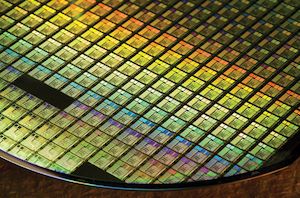
ASML to Ship 30 EUV Scanners in 2019: Faster EUV Tools Coming
ASML said last week that it planned to ship 30 extreme ultraviolet scanners in 2019, up significantly from 2018. The plan is not surprising, as demand for EUV lithography...
17 by Anton Shilov on 1/28/2019
TSMC: First 7nm EUV Chips Taped Out, 5nm Risk Production in Q2 2019
Last week, TSMC made two important announcements concerning its progress with extreme ultraviolet lithography (EUVL). First up, the company has successfully taped out its first customer chip using its...
50 by Anton Shilov on 10/9/2018
Samsung Foundry Updates: 8LPU Added, EUVL on Track for HVM in 2019
Samsung recently hosted its Samsung Foundry Forum 2018 in Japan, where it made several significant foundry announcements. Besides reiterating plans to start high-volume manufacturing (HVM) using extreme ultraviolet lithography...
29 by Anton Shilov on 9/6/2018
Arm and Samsung Extend Artisan POP IP Collaboration to 7LPP and 5LPE Nodes
Arm and Samsung Foundry this week announced plans to extend their collaboration to 7LPP and 5LPE process technologies. Under the terms of the agreement, Arm will offer Samsung Foundry...
23 by Anton Shilov on 7/6/2018
GlobalFoundries Gives 7 nm Capacity Update, Mulls Skipping 5 nm
High-ranking executives of GlobalFoundries this month gave several updates concerning future plans of the contract maker of semiconductors. As it appears, in a bid to provide more tangible advantages...
19 by Anton Shilov on 5/31/2018
Samsung Foundry Roadmap: EUV-Based 7LPP for 2018, 3 nm Incoming
Samsung Foundry this week updated its fabrication technology roadmap, introducing a number of changes and announcing the first details about its 3 nm manufacturing process that is several years...
25 by Anton Shilov on 5/24/2018
TSMC Details 5 nm Process Tech: Aggressive Scaling, But Thin Power and Performance Gains
At a special event last week, TSMC announced the first details about its 5 nm manufacturing technology that it plans to use sometime in 2020. CLN5 will be the...
10 by Anton Shilov on 5/8/2018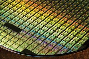
TSMC Kicks Off Volume Production of 7nm Chips
TSMC last week announced that it had started high volume production (HVM) of chips using their first-gen 7 nm (CLN7FF) process technology. The contract maker of semiconductors says it...
63 by Anton Shilov on 4/24/2018
Change of Strategy: A New GlobalFoundries CEO in Dr. Thomas Caulfield
In a surprising move, GlobalFoundries has announced that its CEO is stepping down. Sanjay Jha, who lead the world’s second largest foundry for four years, was in the past...
15 by Anton Shilov on 3/15/2018
TSMC Starts to Build Fab 18: 5 nm, Volume Production in Early 2020
TSMC last week held a groundbreaking ceremony for its Fab 18 phase 1 production facility. The fab will produce chips using TSMC’s 5 nm process starting from early 2020...
27 by Anton Shilov on 1/31/2018


