The Snapdragon 888 vs The Exynos 2100: Cortex-X1 & 5nm - Who Does It Better?
by Andrei Frumusanu on February 8, 2021 3:00 AM EST- Posted in
- Mobile
- Samsung
- Qualcomm
- Smartphones
- SoCs
- Snapdragon 888
- Exynos 2100
Memory Subsystem & Latency: Quite Different
The memory subsystem comparisons for the Snapdragon 888 and Exynos 2100 are very interesting for a few couple of reasons. First of all – these new SoCs are the first to use new higher-frequency LPDDR5-6400 memory, which is 16% faster than that of last year’s LPDRR5-5500 DRAM used in flagship devices.
On the Snapdragon 888 side of things, Qualcomm this generation has said that they have made significant progress in improving memory latency – a point of contention that’s generally been a weak point of the previous few generations, although they always did keep improving things gen-on-gen.
On the Exynos 2100 side, Samsung’s abandonment of their custom cores also means that the SoC is now very different to the Exynos 990. The M5 used to have a fast-path connection between the cores and the memory controllers – exactly how Samsung reimplemented this in the Exynos 2100 will be interesting.
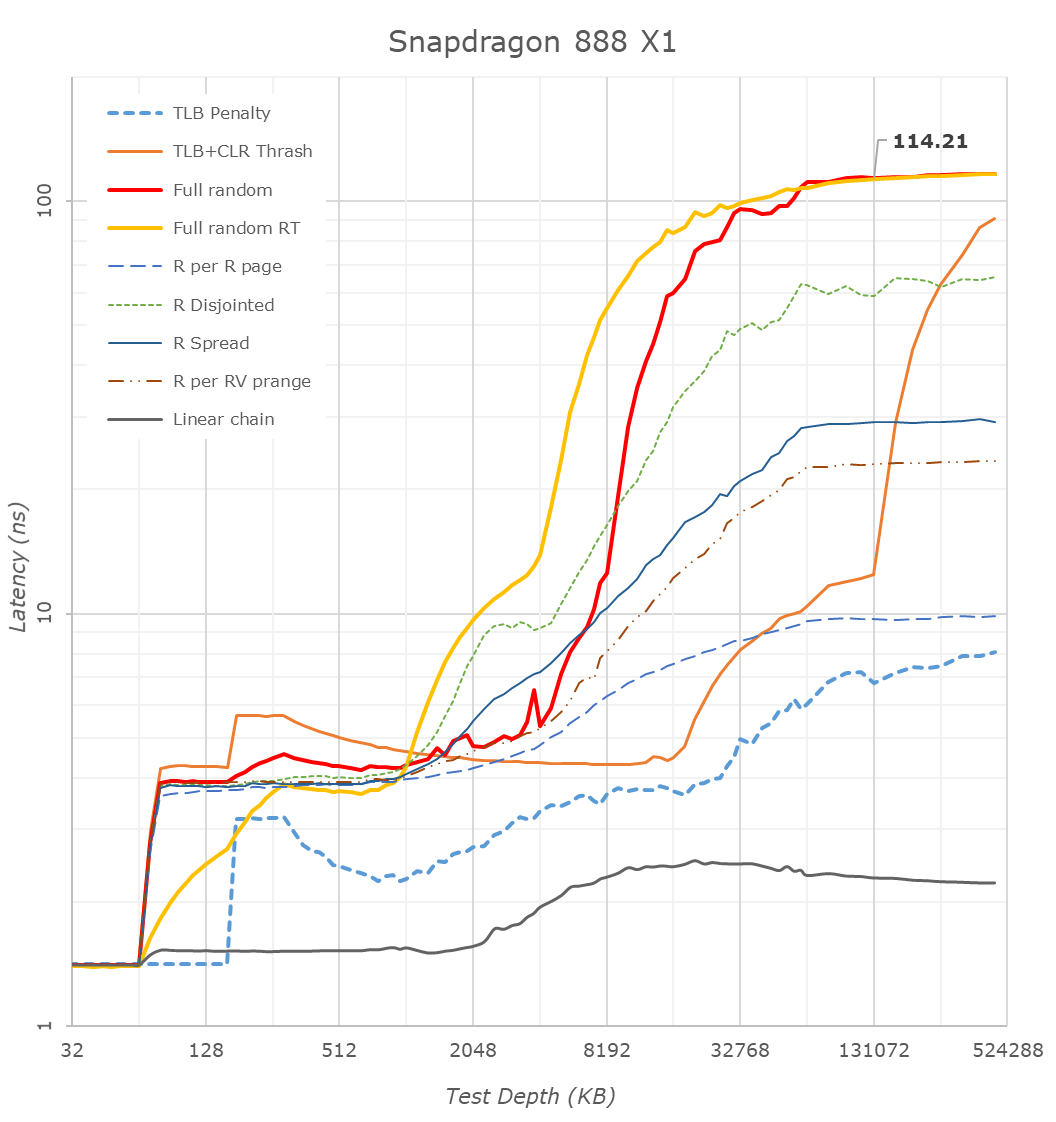
Starting things off with the new Snapdragon 888, we are seeing some very significant changes compared to the Snapdragon 865 last year. Full random memory latency went down from 138ns to 114ns, which is a massive generation gain given that Arm always quotes that 4ns of latency equals 1% of performance.
Samsung’s Exynos 2100 on the other hand doesn’t look as good: At around 136ns at 128MB test depth, this is quite worse than the Snapdragon 888, and actually a regression compared to the Exynos 990 at 131ns.
Looking closer at the cache hierarchies, we’re seeing 64KB of L1 caches for both X1 designs – as expected.
What’s really weird though is the memory patterns of the X1 and A78 cores as they transition from the L2 caches to the L3 caches. Usually, you’d expect a larger latency hump into the 10’s of nanoseconds, however on both the Cortex-X1 and Cortex-A78 on both the Snapdragon and Exynos we’re seeing L3 latencies between 4-6ns which is far faster than any previous generation L3 and DSU design we’ve seen from Arm.
After experimenting a bit with my patterns, the answer to this weird behaviour is quite amazing: Arm is prefetching all these patterns, including the “full random” memory access pattern. My tests here consist of pointer-chasing loops across a given depth of memory, with the pointer-loop being closed and always repeated. Arm seems to have a new temporal prefetcher that recognizes arbitrary memory patterns and will latch onto them and prefetch them in further iterations.
I re-added an alternative full random access pattern test (“Full random RT”) into the graph as alternative data-points. This variant instead of being pointer-chase based, will compute a random target address at runtime before accessing it, meaning it’ll be always a different access pattern on repeated loops of a given memory depth. The curves here aren’t as nice and they aren’t as tight as the pointer-chase variant because it currently doesn’t guarantee that it’ll visit every cache line at a given depth and it also doesn’t guarantee not revisiting a cache line within a test depth loop, which is why some of the latencies are lower than that of the “Full random” pattern – just ignore these parts.
This alternative patterns also more clearly reveals the 512KB versus 1MB L2 cache differences between the Exynos’ X1 core and the Snapdragon X1 core. Both chips have 4MB of L3, which is pretty straightforward to identify.
What’s odd about the Exynos is the linear access latencies. Unlike the Snapdragon whose latency grows at 4MB and remains relatively the same, the Exynos sees a second latency hump around the 10MB depth mark. It’s hard to see here in the other patterns, but it’s also actually present there.
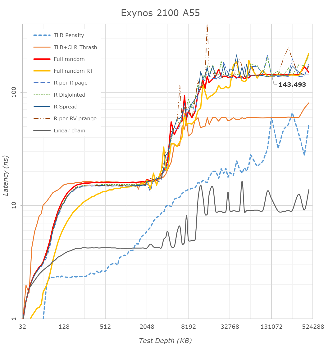
This post-4MB L3 cache hierarchy is actually easier to identify from the perspective of the Cortex-A55 cores. We see a very different pattern between the Exynos 2100 and the Snapdragon 888 here, and again confirms that there’s lowered latencies up until around 10MB depth.
During the announcement of the Exynos 2100, Samsung had mentioned they had improved and included “better cache memory”, which in context of these results seems to be pointing out that they’ve now increased their system level cache from 2MB to 6MB. I’m not 100% sure if it’s 6 or 8MB, but 6 seems to be a safe bet for now.
In these A55 graphs, we also see that Samsung continues to use 64KB L2 caches, while Qualcomm makes use of 128KB implementations. Furthermore, it looks like the Exynos 2100 makes available to the A55 cores the full speed of the memory controllers, while the Snapdragon 888 puts a hard limit on them, and hence the very bad memory latency, similarly to how Apple does the same in their SoCs when just the small cores are active.
Qualcomm seems to have completely removed access of the CPU cluster to the SoC’s system cache, as even the Cortex-A55 cores don’t look to have access to it. This might explain why the CPU memory latency this generation has been greatly improved – as after all, memory traffic had to do one whole hop less this generation. This also in theory would put less pressure on the SLC, and allow the GPU and other blocks to more effectively use its 3MB size.


123 Comments
View All Comments
serendip - Monday, February 8, 2021 - link
I'm interested in what this means for the SD8cx successor. A 30% increase from using one or two X1 cores would be great, I'm using the SQ2 chip and that's fast enough for typical office tasks. That's still not enough to get within striking range of the M1 or even A14. What the heck is in those Firestorms that makes them so fast?On memory subsystems, what are Qualcomm and Samsung doing wrong compared to Apple and HiSilicon? The M1's memory bandwidth is astonishingly high but that's from using custom parts. HiSilicon is doing a great job using standard ARM interconnects.
Agreed on the stupidly high GPU clocking. The SQ2 has a beefy GPU that performs well but it can get hot even in a large tablet form factor. It's time to stop the marketing departments from forcing engineers to chase pointless metrics.
ikjadoon - Monday, February 8, 2021 - link
>What the heck is in those Firestorms that makes them so fast?A trifecta that I share with people because this question comes up so often.
Technical Part 1: https://www.anandtech.com/show/16226/apple-silicon...
Technical Part 2: https://www.anandtech.com/show/16252/mac-mini-appl...
Consumer + Approachable: https://www.youtube.com/watch?v=3SG5e4z-Ygg
Technical Background + More Approachable: https://www.youtube.com/watch?v=cAjarAgf0nI
As Upscaled wrote, "It's not magic. It's good design." And why don't AMD / Intel have these same good designs? The videos above give thorough answers. For example, the last link explains why everyone cares Firestorm (A14) and Lightning (A13) have an 8-wide decode, which is one of many major "better designs" versus competing Arm & x86 CPUs.
ikjadoon - Monday, February 8, 2021 - link
Uh, wait. Delete. I definitely skipped too much of that one. What on Earth is he going on about 1T vs 1C?~~ Consumer + Approachable: https://www.youtube.com/watch?v=3SG5e4z-Ygg ~~
Wow, I'm a little stunned at how bad this Upscaled video is. The Dev Doc + AnandTech are much more reliable.
Nicon0s - Monday, February 8, 2021 - link
LoL, Engadget.He keeps saying multithreading when he means SMT or Hyperthreading(Intel's version of SMT).
ikjadoon - Monday, February 8, 2021 - link
Yes! Never mind 1T / 1C have shown negligence IPC differences in general computing. 1% at best. Please go test an i5-8600K vs an i7-8700K: one has SMT, one does not. Terrible to see the WCCFTech disinformation cycle reach a mainstream audience so quickly.https://www.anandtech.com/show/16261/investigating...
And then he, out of left field, throws up a Cinebench multi-core score: "See? Intel and Apple are actually very close to each other." But, his comparison was the 4+4 M1 vs an 8C Intel...
I wish I could edit comments. I give up on consumer YouTube videos; I saw his earlier interview with RISC's founders and it seemed halfway decent. I'm a fool.
Archer_Legend - Tuesday, February 9, 2021 - link
Don't be offended but I think that what you posted is completely bs.First of all you are comparing arm64 cpus and x86 cpus, second the arm 64 cores used by apple are very arguably faster than the x86 cores of for example a ryzen cpu.
The second thing which I would want to point out is that about the widht of the pipeline, it is not that apple is a genious or intel and amd are stupid: the x86 architecture was built to have a narrowish pipeline and do more cycles in fact the width of the pipeline in intel and amd cpus is as wide as it gets.
Arm arch on the other end lets you use a wider pipeline, however saying using a narrower or wider pipeline is better or not is pointless because performance comes down to how you organise the cpu around that specific pipeline so....
leledumbo - Monday, February 8, 2021 - link
> What the heck is in those Firestorms that makes them so fast?The same thing since A9 again (CMIIW): super wide decoder + super big cache. Apple isn't stingy when it comes to die size and Apple SoCs are always bigger than Snapdragon on the same generation and process node. 4mm^2 difference is huge when we're talking at nm level. What's weird, Exynos is even bigger but can't match these two. No idea what Samsung put there.
Santoval - Tuesday, February 9, 2021 - link
"What's weird, Exynos is even bigger but can't match these two. No idea what Samsung put there."This is probably due to TSMC having a *far* denser 5nm process node compared to Samsung's process 5nm node. Per the article below TSMC's 5nm node tops at 173 million transistors per mm^2 while Samsung's 5nm node reaches only 126.5 MTr/mm^2 (i.e. barely denser than TSMC's second gen 7nm+ node) due to much more, er, "conservative" design choices (Samsung basically just switched from DDB cells in 7nm to SDB cells; the article explains what that means).
What is often not clear is that the quoted transistor densities of each process node are always the *maximum* transistor densities, not the actual transistor densities used to fab a die. For instance Intel have three different 10nm node variants with three different densities, a low, mid and high density variant (ranging I believe from ~55 million to ~100 million transistors per mm^2). The last one is the only one that has been widely reported, the other two were intended for the tech savvy press and audience.
Each Intel 10nm die has a mix of all three libraries, but each design is (obviously) *fixed* with a precise mix of the three. The desktop parts always have a higher percentage of low density cells because these need to clock higher, and vice versa for the mobile parts. Mobile phones are efficiency focused, so their SoCs have the highest percentage of the highest density variant of each process node that is possible (without hindering performance too much).
That is an additional reason their clocks top at ~3 GHz. Since the two SoCs of the article are both mobile SoCs of an almost identical design we can assume a roughly equivalent percentage of the highest density cells each process node maxes out at. Thus, if all else was being equal (including the same iGPU) Samsung's SoC would have a roughly ~27% larger die than TSMC's SoC. That must be the main reason Samsung kept the cache sizes of the X1 and the A55 cores low.
Santoval - Tuesday, February 9, 2021 - link
p.s. Sorry, I forgot the link to the article :https://semiwiki.com/semiconductor-manufacturers/s...
Santoval - Tuesday, February 9, 2021 - link
p.s.2 I just noticed that the Snapdragon 888 is also fabbed with Samsung's 5nm node. While that rendered the comparison between the two SoCs in my above comment moot the other things I pointed out might have some "academic" value regarding process nodes (I have no away to delete the comment anyway..).