The EVGA X299 FTW K Motherboard Review: Dual U.2 Ports
by Joe Shields on January 29, 2018 8:45 AM EST- Posted in
- Motherboards
- Intel
- Killer
- EVGA
- X299
- Basin Falls
- Skylake-X
- Kaby Lake-X
Visual Inspection
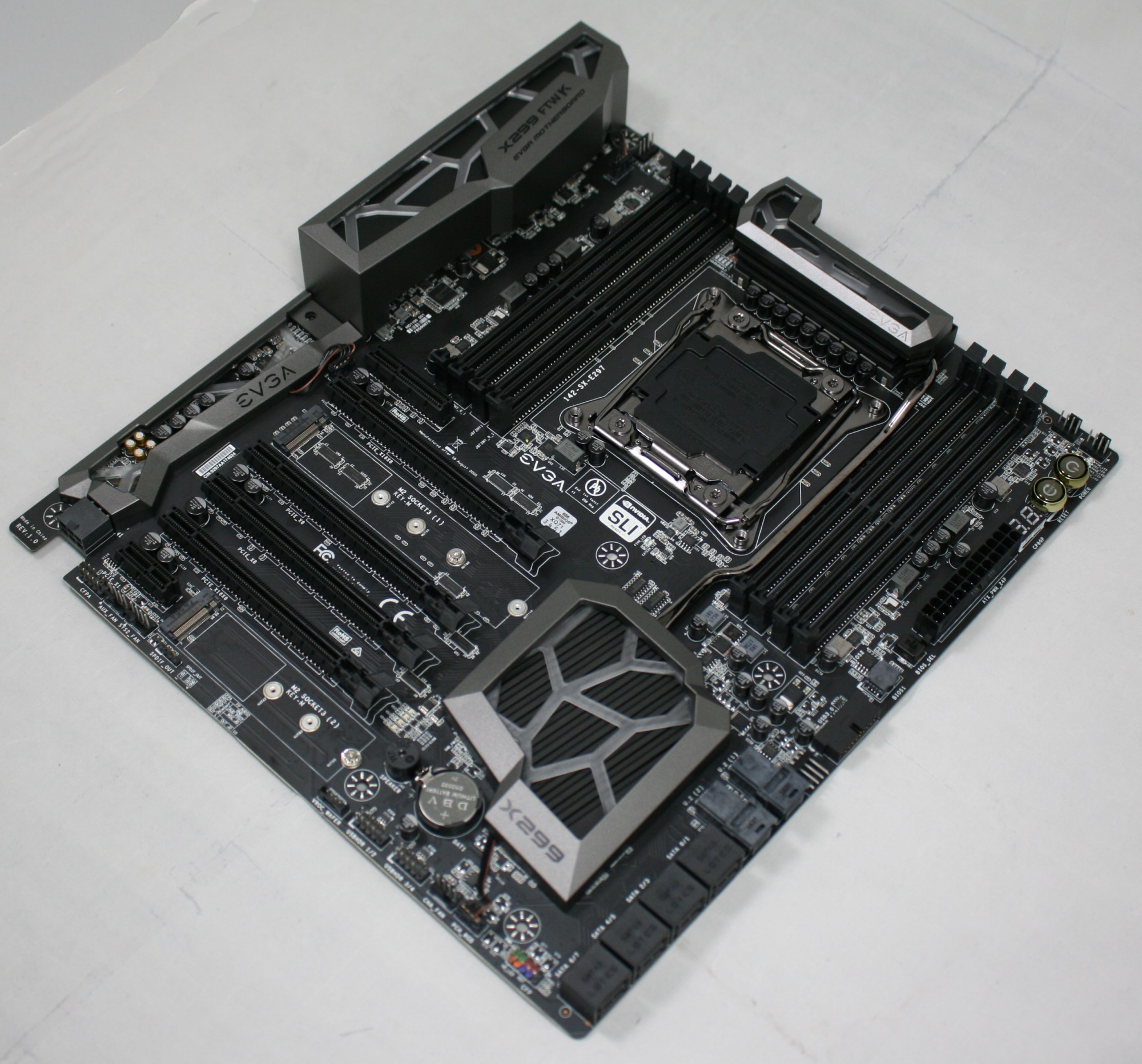
The EVGA X299 FTW K is an all black motherboard, with shrouding hiding the back panel IO and the audio bits further down the board. An item to note here is EVGA did not install the shrouding: it is something the user will have to do. The board uses all black memory and PCIe slots, designed to match the PCB. The chipset and power delivery heatsinks, black with a silver outline like the rear panel shroud, are attached via heat pipe and help share the load. We did not record any issues with this setup during stock operation, nor overclocking.
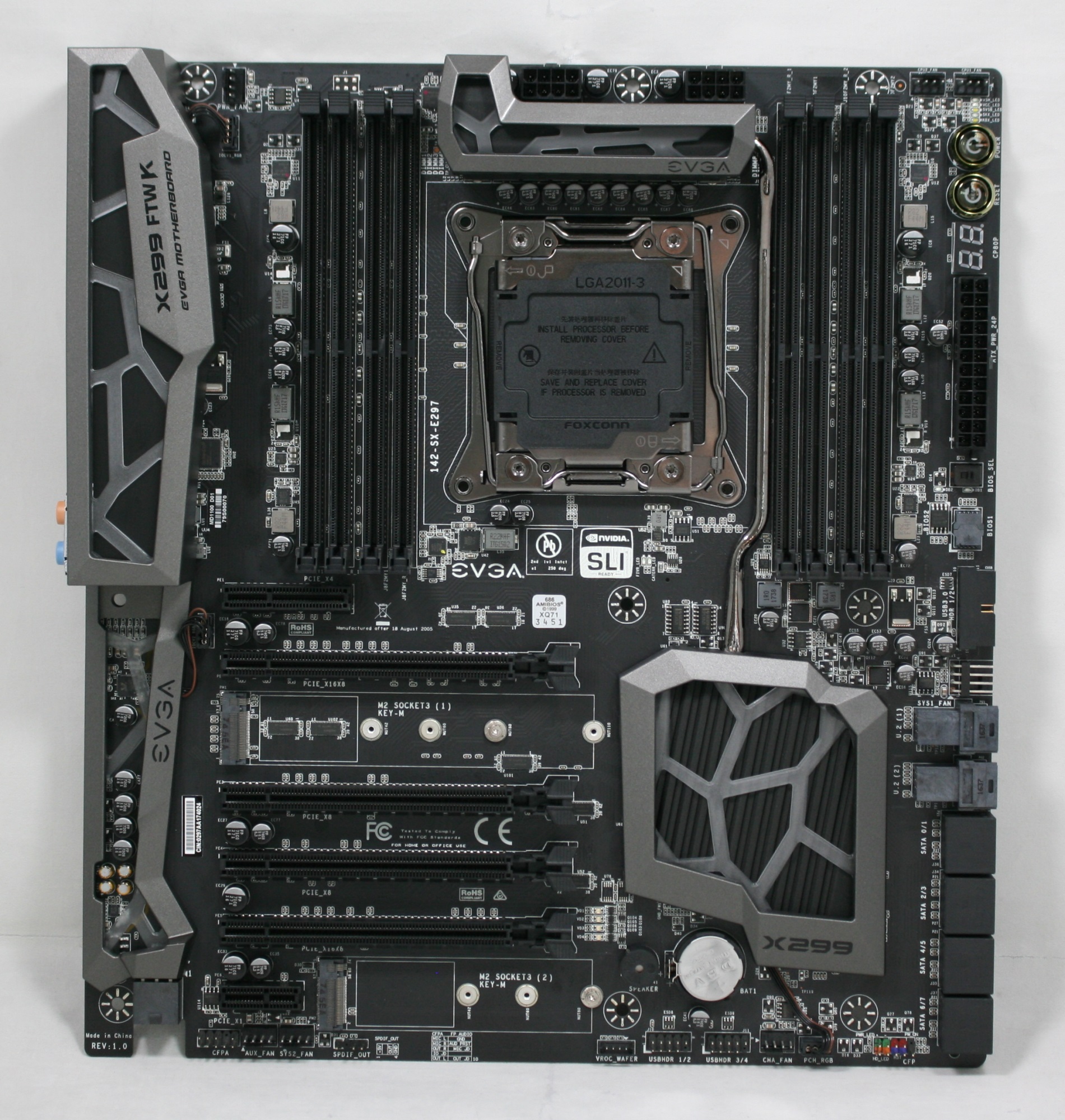
It is worth noting that due to the shroud, a longer-than-normal screw will be needed in the 9 o'clock screw position. The shroud makes the board thicker and typical motherboard screws will not reach. EVGA does not supply these screws.
Onboard lighting is found through the audio and panel shroud, as well as the chipset heatsink on the production model. A few months ago when we first saw the board, the power delivery heatsink was lit up as well. The onboard LEDs can be controlled through the EVGA E-Leet software and offers four modes: static, on/off, rainbow, and breathing. Compared to other motherboards, this is a fewer number of options. There is also an RGB LED controller header at the bottom part of the board.

As far as fan headers go, the FTW K has a total of seven 4-pin headers. The two CPU headers, located in the upper right-hand corner, are able to control attached fans via PWM only. The remaining five headers scattered around the board in strategic locations support both PWM and DC control. All headers are designed to deliver 1A (12W) to the header. I would have liked to see at least one high-power header as most of the other boards in this class have them.
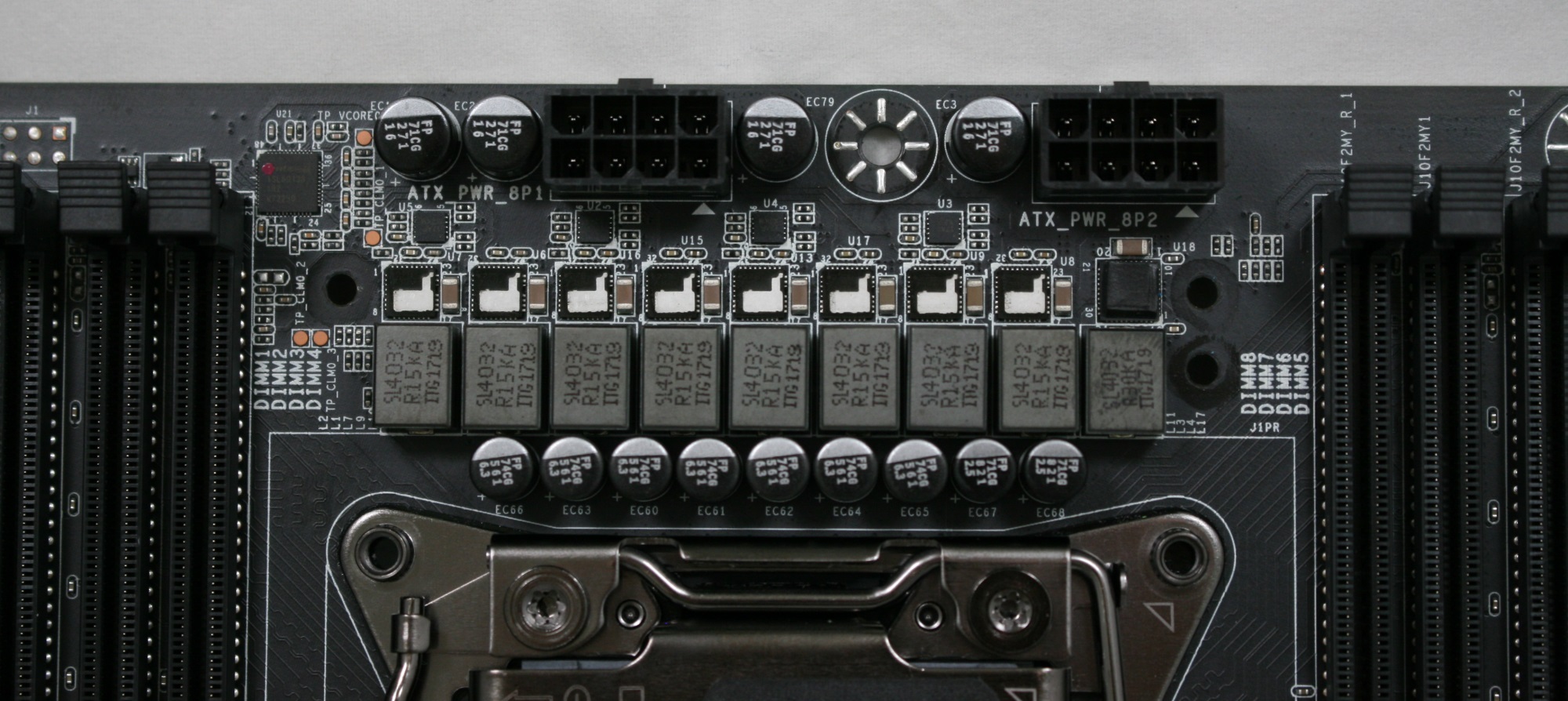
The socket area is fairly clean with the VRMs lining the top side. The FTW K has a 10 phase power delivery, with eight dedicated to Vcore and one each going to System Agent and VCCIO. The VRM uses Intersil ISL69138 and ISL99227B MOSFETs for Vcore and VCCIN. The VSA uses ISL66133 and ISL99227 for the DRAM. Delivering power to the VRMs is are two 8-pin EPS connectors; with only one is required for most conditions. The rest of the power is fed from the 24-pin ATX connector. During our testing the VRMs did get warm, but nothing that caused throttling in our testing, even at peak overclock.
DRAM support on the FTW K is up to 128GB, with speeds supported up to DDR4-4000 in quad channel mode with Skylake-X CPUs. For Kaby Lake-X, speeds up to DDR4-4133 are supported.
The right edge of the board has a lot going on. On the far right of this image below, we are able to see the CPU fan headers and are a couple of informational LEDs. When powered, there are four lights that will pop up: VSM in yellow, VCC in red, 5VSB in white, and either a Skylake-X light in yellow, or a Kaby Lake-X light in white depending on which processor is installed. Note when the indicators are lit up it simply means the voltage is detected, but does not mean it is in spec. Next to these, EVGA has placed gold colored power and reset buttons with the reset button LED doubling as an onboard HDD LED indicator. These buttons are good for open air cases or just handy to have when working inside of the case. To the left of that is the debug LED and 24-pin ATX power connector. Next, we are able to see the BIOS selector switch as well as one removable BIOS chip and a second soldered to the board. Then we get a front panel USB 3.0 header as well as one of the chassis fan headers. Last are the two U.2 connectors as well as eight SATA ports.
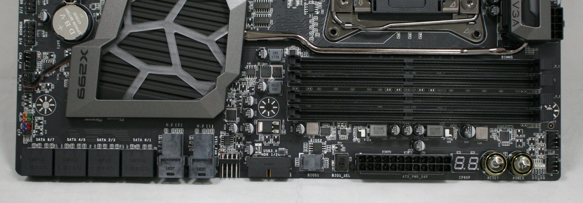
Below we see a closeup of those eight SATA ports and the two U.2 connectors. All eight SATA ports are use the chipset for its bandwidth, with SATA ports 0/1 being disabled when using a SATA based SSD in the lower M.2 slot. The U.2 ports are only active when using a 44-lane CPU.

The bottom edge of the board has several headers across its length. Unique about this board is the supplemental 6-pin PCIe power connector on the far left, used to give additional power to multiple GPUs. The 6-pin PCIe power connector is offset from the bottom of the board and will help with cable management. Along side this are additional USB headers, chassis fan headers, and an Intel VROC header.
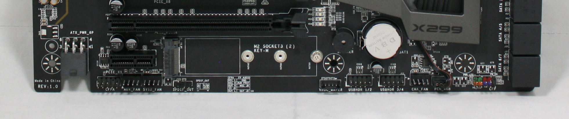
The bottom half of the board contains the audio bits on the left, PCIe area in the middle, then the RGB LED chipset heatsink. The audio section is isolated from the board and uses Nichicon audio caps for a warmer sound. The Realtek ALC1150 codec is not covered with EMI protection and is partially visible through the design on the shroud, just to the left of the "A" in EVGA. The ALC1150 codec is a carry over from Realtek's previous generation audio, while many mid-range or higher boards have the latest ALC1220 codec.

There are a total of six PCIe slots on the board with four full-length slots sourced from the CPU. There are two other slots: an x4 slot up top and an x1 slot on the bottom, both fed by the chipset. The board both SLI and Crossfire, although only up to 3-way. There is a lot of lane sharing going on between these PCIe slots; for example, the top full-length slot (PCIe 2) shares bandwidth with the second full-length slot (PCIe 3). The fourth full-length slot (PCIe 5) shares bandwidth the slot above it, PCIe 4. This can make for some confusing slot breakdowns. With a two card configuration, the video cards will sit in PCIe 2 and PCIe 5 while three card configurations will use PCIe 2, 3, and 5. Single card configurations should use the top full-length slot (PCIe 2).
So despite the motherboard allowing for x8/x8/x8/x8 in the full length slots, for whatever reason EVGA has only qualified this motherboard for 3-way multi-GPU action. With single slot GPUs, or high-end GPUs with single-slot sized water blocks in a cooling loop, this motherboard should have been able to do four-way. It is likely that the Crossfire will work in 4-way, although SLI has to have the correct keys in the firmware installed to work, which requires certification.
The M.2 slots sit between the first two full-length PCIe slots and supports up to 110mm PCIe 3.0 x4 SSD modules, powered by the CPU, while the second is at the bottom supports up to an 80mm PCIe 3.0 x4 SSD modules, and SATA modules, but powered by the chipset. If a SATA module is installed to this second slot, the physical SATA ports 0/1 will be disabled.
Below is a simplified list of how the PCIe slots will work with each family of CPUs (talking PCIe lanes) when multiple cards are used (the "@" symbol is used to show slot preference for the configuration):
| EVGA X299 FTW K CPU PCIe Layout | |||||||
| 44-Lane 1/2-Way |
44-Lane 3-Way |
28-Lane 1/2-Way |
28-Lane 3-Way |
16-Lane 1-Way |
16-Lane 2-Way |
||
| PCIe 2 | @x16 | @x8 | @x16 | @x8 | @x8 | @x8 | |
| PCIe 3 | - | @x8 | - | @x8 | - | - | |
| PCIe 4 | - | - | - | - | - | - | |
| PCIe 5 | @x16 | @x16 | @x8 | @x8 | - | @x8 | x4* |
| SLI | Yes | Yes | Yes | Yes | - | Yes | No |
| M.2 110mm | x4 | x4 | x4 | x4 | x4 | No | x4* |
| U.2 | Yes | Yes | No | No | No | No | |
* With a 16-lane CPU, PCIe 5 will be in x4 mode if an M.2 drive is installed in the 110mm slot.
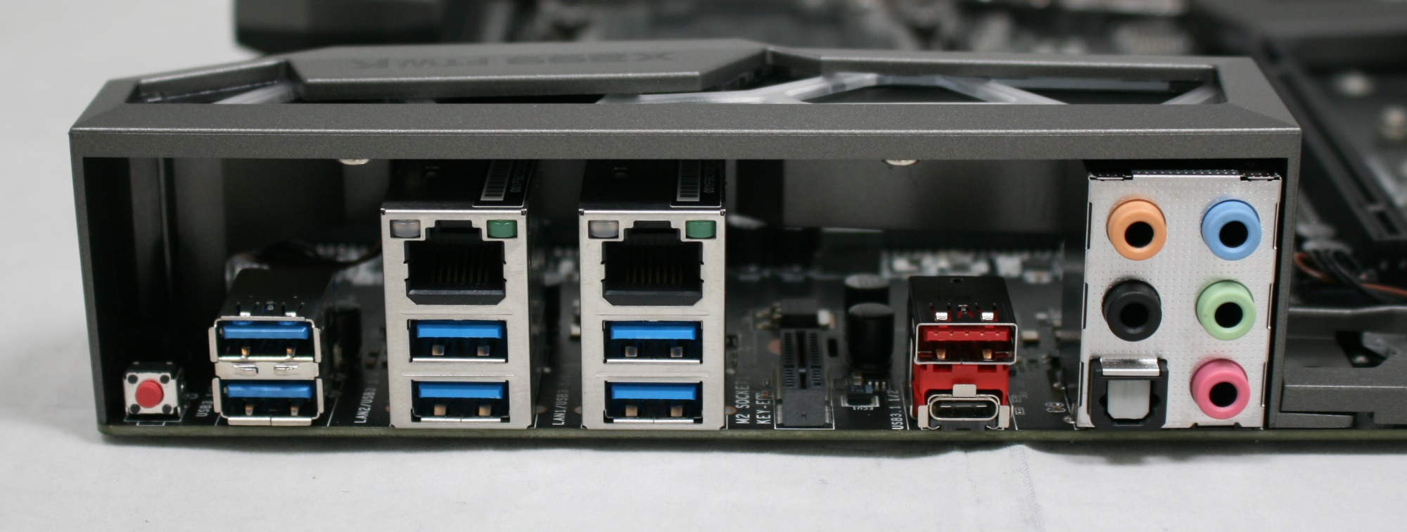
The back panel IO consists of:
- CMOS reset button
- 6 x USB 3.1 (5 Gbps) ports
- 1 x Intel I219-V Gigabit NIC
- 1 x Killer E2500 Gigabit NIC
- 2 x USB 3.1 (10 Gbps) ports Type-A and Type-C
- 5 plug audio stack with SPDIF output
- 1 x Vertical M.2 Key E slot


In the Box
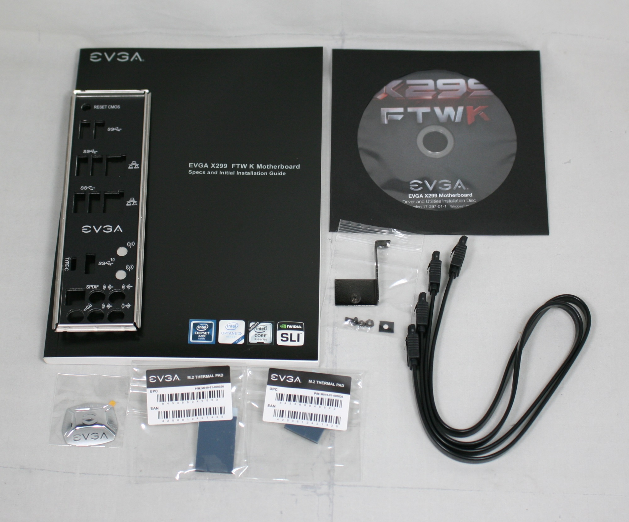
The EVGA FTW-K has one of the most sparse set of included accessories I have seen. But with that said, it does include what you need to get started.
We get the following:
- Driver Disk
- Specs and Installation Guide
- Rear IO Plate
- 2 x SATA 6 Gbps Cables
- 2 x Thermal Pads for M.2 devices
- EVGA sticker


23 Comments
View All Comments
jordanclock - Monday, January 29, 2018 - link
Any chance we could see comparison numbers on the Intel and Killer NICs?Flunk - Monday, January 29, 2018 - link
There is almost no difference, type "intel vs killer nic" into Google. It's been done to death.jordanclock - Monday, January 29, 2018 - link
By that logic, they shouldn't bother including half their benchmarks for motherboards because they are almost always to same for a given chipset.My interest is in this particular motherboards implementation of the dual NICs.
Ian Cutress - Monday, January 29, 2018 - link
Aside from doing a peak throughput test, we're looking into doing something more substantial for NIC testing. Still a WIPjordanclock - Monday, January 29, 2018 - link
Awesome! Glad you're looking to do something more meaningful than peak throughput. It's kind of like the average FPS of networking, in that it gets a lot of attention but isn't the most useful number.ImSpartacus - Monday, January 29, 2018 - link
Whew, I'm glad there's finally a mobo with two u.2 ports.It's so annoying to have all of these u.2 drives without the ability to use more than one at a time!
bug77 - Monday, January 29, 2018 - link
Ha, I was just thinking the same thing when I read the article :PYuriman - Monday, January 29, 2018 - link
Maybe it's just me, but I find those heatsinks pretty ugly.JoeyJoJo123 - Monday, January 29, 2018 - link
It's supposed to align with their For The Win 3 (FTW3) series video cards styling.http://hexus.net/media/uploaded/2017/5/9656d308-25...
It's no different than MSI doing a similar red/black dragon scheme that they've done with their video cards to their motherboards.
bug77 - Monday, January 29, 2018 - link
I find this type of comment pretty useless.No one design choice will ever appeal to everyone. And a chameleonic or customizable look hasn't been done yet, so that comment really brings nothing to the discussion.
It's ok to point out fugly board, so the manufacturer knows not to do that again, but that's far from the case here.