Original Link: https://www.anandtech.com/show/4332/vias-quadcore-nano-gets-bigger
VIA's QuadCore: Nano Gets Bigger
by Anand Lal Shimpi on May 12, 2011 3:01 AM ESTTwo days ago I flew out to VIA's Centaur headquarters in Austin, Texas to be briefed on a new CPU. When I wrote about VIA's Dual-Core Nano I expected the next time we heard from VIA about CPUs to be about its next-generation microprocessor architecture. While Nano still holds a performance advantage over Atom and Bobcat, it's still missing a number of key architectural innovations that both Intel and AMD have adopted in their current generation hardware (e.g. GPU integration, power gating).
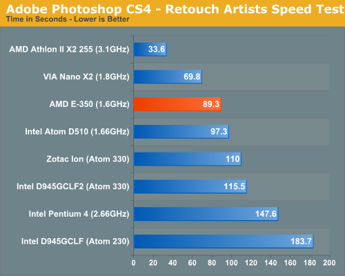
VIA's dual-core Nano, faster than AMD's E-350 and Intel's Atom
Much to my surprise, the meeting wasn't about VIA's next-generation microprocessor architecture but rather the last hurrah for Nano: a quad-core version simply called the VIA QuadCore.
VIA's QuadCore architecture is nothing too surprising. At a high level the chip is composed of two dual-core die connected by a shared 1333MHz FSB, very similar to the old dual-core Pentium D processors. Each dual-core die has two 1MB independent L2 caches, for a total of 4MB of L2 on-package.
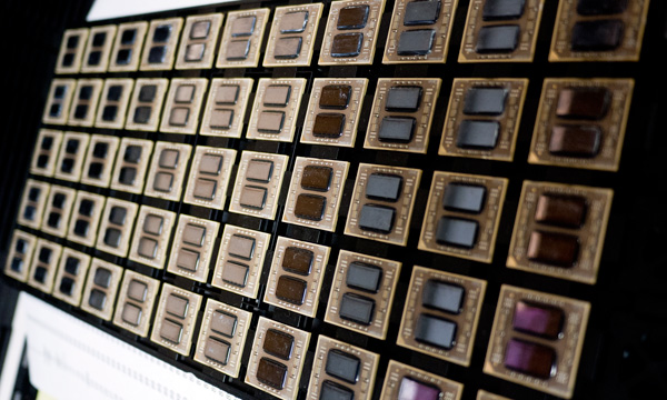
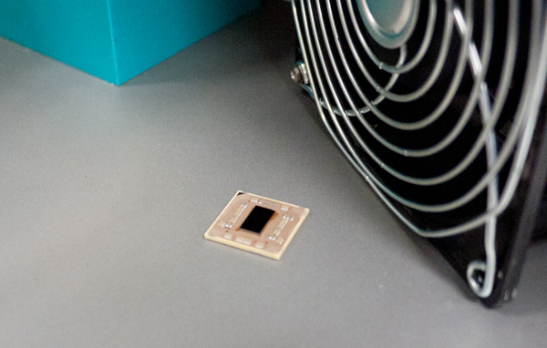
VIA's QuadCore, in production today
Going a little deeper there's an AMD-like 64KB L1 instruction and 64KB L1 data cache per core. The Nano is of course fully 64-bit x86 compatible, supporting up to SSE4. Each core is a 3-issue out-of-order design, giving it a general throughput and performance advantage over Intel's Atom and AMD's Bobcat. Remember that Atom is a 2-issue in-order architecture and Bobcat is 2-issue out-of-order. The wider front end for Nano gives VIA the ability to perform well in more complex workloads.
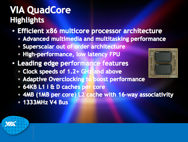
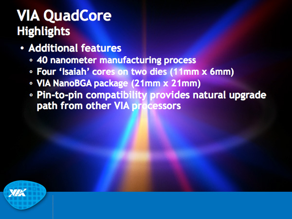
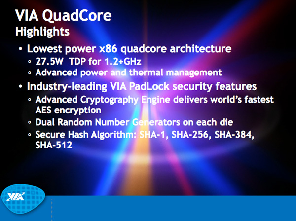
In the past power consumption has been an issue for VIA's Nano, however the QuadCore is built on a 40nm process which helps reel in power consumption. At 1.2GHz, VIA's QuadCore still carries a 27W TDP. Add another 5W for the integrated graphics chipset and you're talking about 32W, nearly double of AMD's dual-core E-350 Brazos platform. VIA claims that at lower clock speeds it can significantly reduce TDP, however the 1.2GHz QuadCore is the only part being announced today.
VIA is calling the 1.2GHz part a 1.2GHz+ QuadCore since it can use available TDP headroom to overclock itself by up to another two bins (133MHz per bin - 1.46GHz max). The chip doesn't support power gating, just aggressive clock gating.
Like all Nano parts, the QuadCore features a hardware AES encryption engine. VIA has added support for SHA-384 and SHA-512 as well.
Although there are still a considerable number of dual-core platforms sold in the market today, designs with four beefy processor cores seem to be where the world as a whole is headed. With its 2011 15/17-inch MacBook Pro and iMac updates, Apple no longer offers a dual-core option in those systems. By the time we move to 22nm I wouldn't be too surprised if the 13-inch MacBook Pro was quad-core only as well.
VIA moving to four cores makes sense and the QuadCore design was an obvious step. Even Intel used a dual-die approach to make the most of its existing microprocessor design before starting from scratch for Nehalem.
As odd as it sounds, VIA's QuadCore actually has a small but viable position in the market. At 27.5W the TDP is too high for a tablet like the iPad, and its performance will be too low to compete with ultra portable Sandy Bridge designs. What VIA could offer however is a a higher performing alternative to Brazos but at a better price than an ultraportable Sandy Bridge notebook.
The bigger issue VIA has to face is the lack of OEM adoption. The QuadCore will launch with whitebox and motherboard designs, not with slick design wins from companies like ASUS or Samsung. With less than 1% of the x86 market, VIA can't command the sort of attention that Intel or even AMD can. That being said, I do believe there's a small window of opportunity here. A clever OEM could put out a system priced similarly to a Brazos (if not lower than), with better performance based on VIA's QuadCore. I haven't looked at the current state of VIA's graphics drivers but when we previewed the dual-core Nano I came away pleasantly surprised. I suspect there will still be issues there going forward, but I remember something an old friend once told me: there are no bad products, just bad pricing. At the right price, in the right system, VIA's QuadCore could work.
The Tour
While this trip to Centaur wasn't my first visit to Austin, it was the first time I had ever visited VIA's x86 CPU division. VIA acquired Centaur 12 years ago, Glenn Henry has been there since the beginning - back when the company was made up of only 4 people.
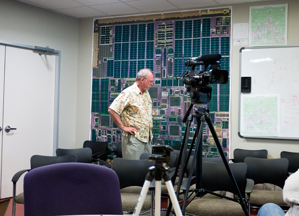
Centaur's Glenn Henry in front of a giant dual-core Nano die shot
Glenn took us all on a tour of Centaur. The company itself has 101 employees, a number that grew from 70 at the time of the VIA acquisition. Glen insists that in order to compete in this market with much more powerful competitors (AMD:Centaur::Intel:AMD) his operation has to be lean and efficient. Everyone likes to say that, but Glen actually showed me proof.
When designing a microprocessor you don't just come up with an architecture and hope it works. You do tons of simulation. First you simulate in software. You build up a C model of parts of your architecture or the entire architecture if possible and run it against datasets. This is how you determine things like cache sizes, balance of resources, and model even more fundamental architectural decisions. When you get further along you'll actually simulate the hardware on large FPGAs or other systems with similar functionality. The idea at this point is less about performance validation but just functional validation. The road to manufacturing is expensive (silicon masks cost a lot of money) and time intensive (from tapeout to first silicon is at least 2 months), so you want to figure out as much about your chip's performance and functionality/bugs ahead of time.
Visit any chip company and you'll find a server farm. Dozens if not hundreds of networked PCs all designed to do simulation and validation tests on chip designs. Intel, AMD, NVIDIA, they've all got them. I remember visiting NVIDIA's validation labs and being told that they are limited by the amount of physical power they can get to the lab so each server upgrade has to provide better power efficiency.
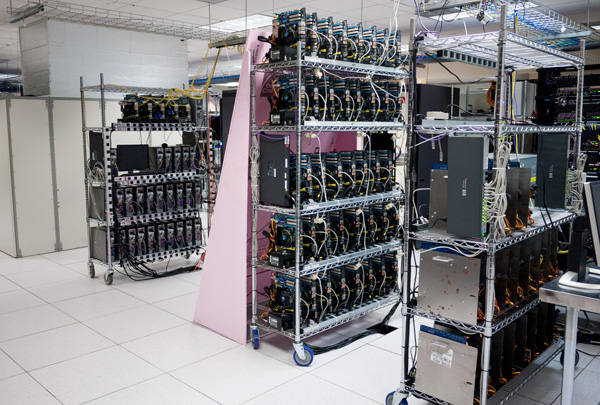
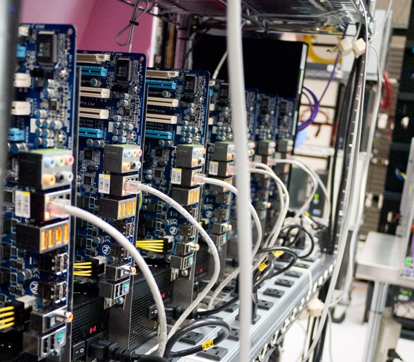
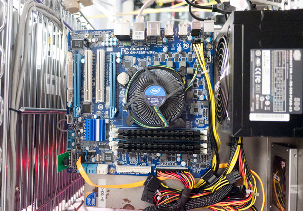
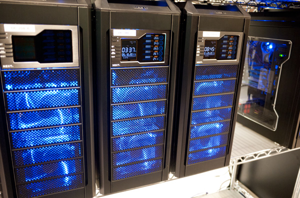
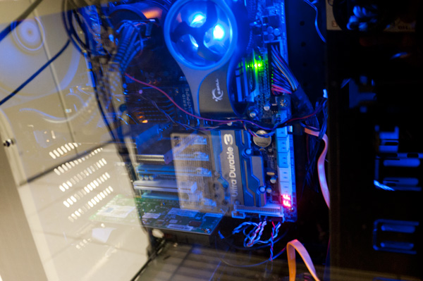
Glen took me on a tour of Centaur's simulation lab. To say it was a different experience would be an understatement. While some machines were racked, there were a lot of desktop motherboards running Core i5s and Core i7s running out of cases:
The systems that were in cases were water cooled Core i7s, overclocked to 5GHz. There are two folks at Centaur who build each and every one of these machines, and overclock them. You and I know that overclocking both Nehalem and Sandy Bridge results in much better performance for the same dollar amount, but this is the first time I've seen overclocking used to speed up the simulation of microprocessors.
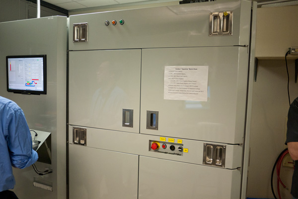
There are similar efforts made all over Centaur. If something can be built more cheaply than it can be bought, Centaur takes the more affordable route. Even Centaur's ovens used for thermal stress testing use a lot of Centaur-built components in order to reduce their total purchase cost to one fifth of what they would be.
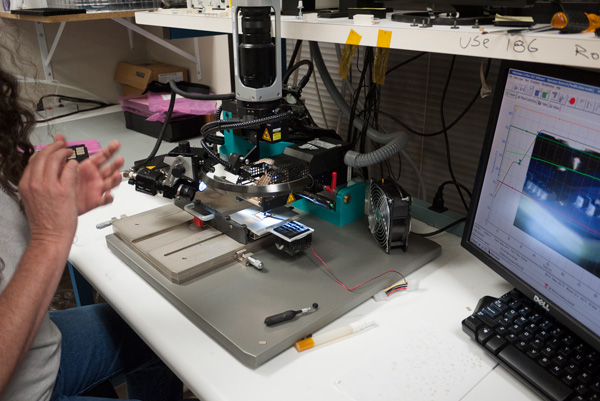
While Centaur didn't have a wafer saw on hand, it can solder and package its own die. This station was used to package a dual-core Nano while a number of journalists watched:
I do wonder about Centaur's future especially as its message of low power operation is now front and center with the current smartphone revolution taking place. In the early days Centaur had to convince users that power was important and that performance was good enough. These days the convincing isn't necessary; it's more about execution, vendor relationships and all of the other pieces of the integrated puzzle. Can VIA and Centaur play a more significant role in the future? The ingredients are there, the question is whether or not VIA is willing to take the risk to give it a try.

