Intel and Micron Develop Hybrid Memory Cube, Stacked DRAM is Coming
by Anand Lal Shimpi on September 15, 2011 1:10 PM ESTDuring the final keynote of IDF, Intel's Justin Rattner demonstrated a new stacked DRAM technology called the Hybrid Memory Cube (HMC). The need is clear: if CPU performance is to continue to scale, there can't be any bottlenecks preventing that scaling from happening. Memory bandwidth has always been a bottleneck we've been worried about as an industry. Ten years ago the worry was that parallel DRAM interfaces wouldn't be able to cut it. Thankfully through tons of innovation we're able to put down 128-bit wide DRAM paths on mainstream motherboards and use some very high speed memories attached to it. What many thought couldn't be done became commonplace and affordable. The question is where do we go from there? DRAM frequencies won't scale forever and continually widening buses isn't exactly feasible.
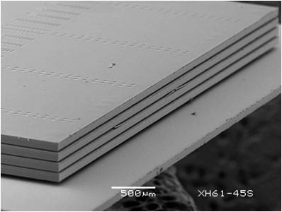
Intel and Micron came up with an idea. Take a DRAM stack and mate it with a logic process (think CPU process, not DRAM fabs) layer for buffering and routing and you can deliver a very high bandwidth, low power DRAM. The buffer layer is actually key here because it helps solve the problem of routing pins to multiple DRAM die. By using a more advanced logic process it's likely that the problem of routing all of that data is made easier. It's this stacked DRAM + logic that's called the Hybrid Memory Cube.
The prototype these two companies developed is good for data rates of up to 1 terabit per second of bandwidth. Intel claims that the technology can deliver bandwidth at 7x the power efficiency of the most efficient DDR3 available today.
The big concern here is obviously manufacturing and by extension, cost. But as with all technologies in this industry, if there's a need, they'll find a way.


19 Comments
View All Comments
prophet001 - Friday, September 16, 2011 - link
Help me understand. Isn't 1 Terabit per second a phenomenal data transfer rate? I understand that there's probably not much need to consume that much data in any system at this point but part of the article is about opening the door for future technology. I thought it was a rather substantial advancement.Klinky1984 - Friday, September 16, 2011 - link
Actually 1 terabit/sec & greater speeds are already being used by high-end GPUs. Though it's not done as "efficiently" as this tech could possibly do it.DanNeely - Friday, September 16, 2011 - link
Stuff I've read indicates that intel intends to put it in their next CPUs as video ram. The silicon connect layer means it has to be an SOC style package because you can't customize layout like you can with a PCB for each vendor.Saltticus - Thursday, September 15, 2011 - link
All this new technology gets me so excited!PS. I believe the word 'parallel' is misspelled in the middle of the first paragraph.
mlkmade - Thursday, September 15, 2011 - link
Why no news on SB-E? We hardly know anything "official" about it and its supposed to come out in 2 months.Usually, at IDFs in the past, Intel has always spilled the beans on the most the new/impeding uARCHs that will launch shortly after the show..
MODist - Thursday, September 15, 2011 - link
Finally 3D technology is getting exciting.toyotabedzrock - Friday, September 16, 2011 - link
I read this and can't help but notice the similarities to FBDIMM and RDRAM.They need to just face up the fact they will have to pay the licensing fee for DDR4 and DDR5.
stephenbrooks - Sunday, September 25, 2011 - link
Does this logic layer tie in well with the idea of an optical CPU-RAM path? E.g. the silicon lasers could be put on the RAM's logic layer in the end.DDR4 - Thursday, February 2, 2012 - link
The memory chips will each take the same amount of voltage as on a non-stacked module, thus it increases the power intake.Will this type of module require a heat sink?