NVIDIA's GeForce GTX 550 Ti: Coming Up Short At $150
by Ryan Smith on March 15, 2011 9:00 AM ESTThroughout the lifetime of the 400 series, NVIDIA launched 4 GPUs: GF100, GF104, GF106, and GF108. Launched in that respective order, they became the GTX 480, GTX 460, GTS 450, and GT 430. One of the interesting things from the resulting products was that with the exception of the GT 430, NVIDIA launched each product with a less than fully populated GPU, shipping with different configurations of disabled shaders, ROPs, and memory controllers. NVIDIA has never fully opened up on why this is – be it for technical or competitive reasons – but ultimately GF100/GF104/GF106 never had the chance to fully spread their wings as 400 series parts.
It’s the 500 series that has corrected this. Starting with the GTX 580 in November of 2010, NVIDIA has been launching GPUs built on a refined transistor design with all functional units enabled. Coupled with a hearty boost in clockspeed, the performance gains have been quite notable given that this is still on the same 40nm process with a die size effectively unchanged. Thus after GTX 560 and the GF114 GPU in January, it’s time for the 3rd and final of the originally scaled down Fermi GPUs to be set loose: GF106. Reincarnated as GF116, it’s the fully enabled GPU that powers NVIDIA’s latest card, the GeForce GTX 550 Ti.
| GTX 560 Ti | GTX 460 768MB | GTX 550 Ti | GTS 450 | |
| Stream Processors | 384 | 336 | 192 | 192 |
| Texture Address / Filtering | 64/64 | 56/56 | 32/32 | 32/32 |
| ROPs | 32 | 24 | 24 | 16 |
| Core Clock | 822MHz | 675MHz | 900MHz | 783MHz |
| Shader Clock | 1644MHz | 1350MHz | 1800MHz | 1566MHz |
| Memory Clock | 1002Mhz (4.008GHz data rate) GDDR5 | 900Mhz (3.6GHz data rate) GDDR5 | 1026Mhz (4.104GHz data rate) GDDR5 | 902Mhz (3.608GHz data rate) GDDR5 |
| Memory Bus Width | 256-bit | 192-bit | 192-bit | 128-bit |
| RAM | 1GB | 768MB | 1GB | 1GB |
| FP64 | 1/12 FP32 | 1/12 FP32 | 1/12 FP32 | 1/12 FP32 |
| Transistor Count | 1.95B | 1.95B | 1.17B | 1.17B |
| Manufacturing Process | TSMC 40nm | TSMC 40nm | TSMC 40nm | TSMC 40nm |
| Price Point | $249 | ~$130 | $149 | ~$90 |
Out of the 3 scaled down 400 series cards, GTS 450 was always the most unique in how NVIDIA went about it. GF100 and GF104 disabled Streaming Multiprocessors (SMs), which housed and therefore cut down on the number of CUDA Cores/SPs and Polymorph Engines. However for GTS 450, NVIDIA instead chose to disable a ROP/memory block, giving GTS 450 the full shader/geometry performance of GF106 (on paper at least), but reduced memory bandwidth, L2 cache, and ROP throughput. We’ve always wondered why NVIDIA built a lower-performance/high-volume GPU with an odd number of memory blocks and what the immediate implications would be of disabling one of those blocks. Now we get to find out.
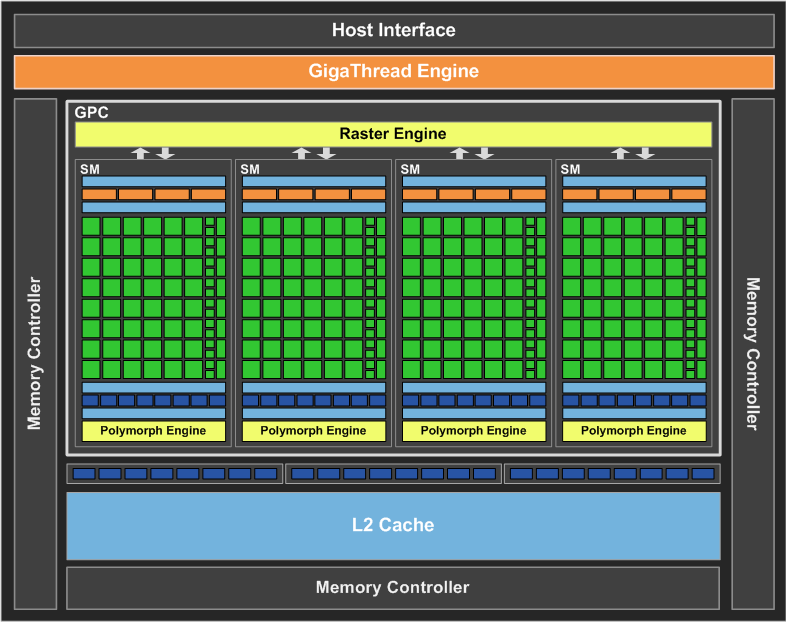
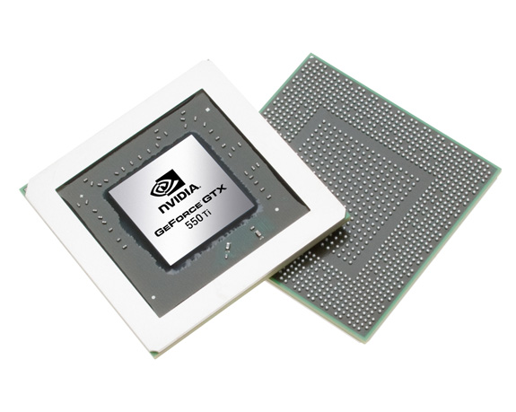
Launching today is the GTX 550 Ti, which features the GF116 GPU. As with GF114 before it, GF116 is a slight process tweak over GF106, using a new selection of transistors in order to reduce leakage, increase clocks, and to improve the card’s performance per watt. With these changes in hand NVIDIA has fully unlocked GF106/GF116 for the first time, giving GTX 550 Ti the responsibility of being the first fully enabled part: 192 CUDA cores is paired with 24 ROPs, 32 texture units, 384KB of L2 cache, a 192-bit memory bus, and 1GB of GDDR5.
The GTX 550 Ti will be shipping at a core clock of 900MHz and a memory clock of 1026MHz (4104MHz data rate), the odd memory speed being due to NVIDIA’s quirky PLLs. If you recall, GTS 450 was clocked at 783MHz core and 902MHz memory, giving the GTX 550 Ti an immediate 117MHz (15%) core clock and 124MHz (14%) memory clock advantage, with the latter coming on top of an additional 50% memory bandwidth advantage due to the wider memory bus (192-bit vs. 128-bit). NVIDIA puts the TDP at 116W, 10W over GTS 450. GF116 remains effectively unchanged from GF106, giving it a transistor count of 1.17B, with the power difference coming down to higher clocks and the additional functional units that have been enabled.
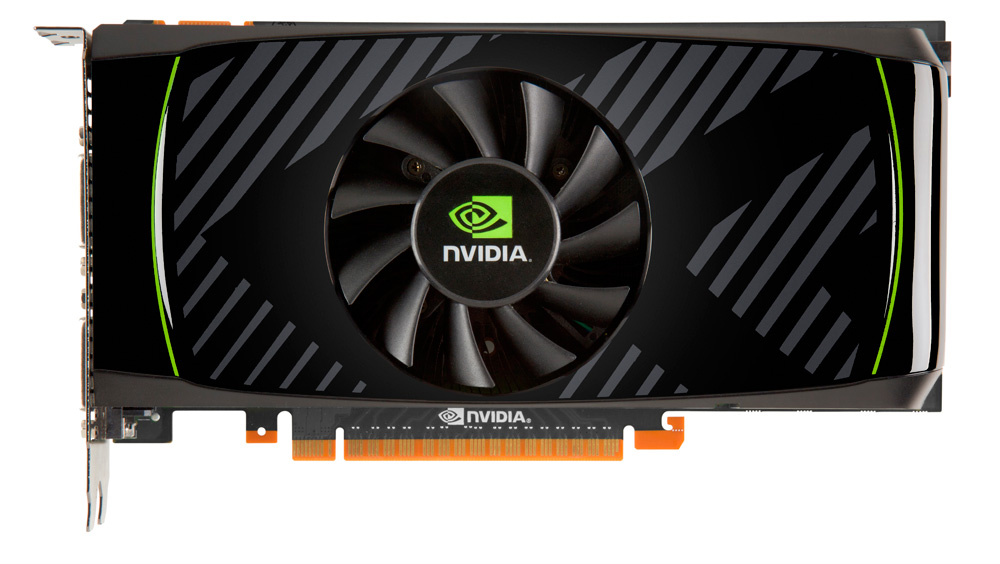
Unlike the GTS 450 launch, GTX 550 Ti is a more laid back affair for NVIDIA – admittedly this is more often a bad sign than it is a good one when it comes to gauging their confidence in a product. As a result they are not sampling any reference cards to reviewers, instead leaving that up to their board partners. As with GF104/GF114, GF116 is pin compatible with GF106, meaning partners can mostly reuse GTS 450 designs; they need only reorganize the PCB to handle a 192bit bus along with meeting the slightly higher power and cooling requirements. As a result a number of custom designs and overclocked cards will be launching right out of the gate, and you’re unlikely to ever see a reference card. Today we’re looking at Zotac’s GeForce GTX 550 Ti AMP, a factory overclocked card that pushes the core and memory clocks to 1000MHz and 1100MHz respectively. The MSRP on the GTX 550 Ti is $149 - $20 more than where GTS 450 launched at – while overclocked cards such as the Zotac model will go for more.
As was the case with the GTS 450, NVIDIA is primarily targeting the GTX 550 Ti towards buyers looking at driving 1680x1050 and smaller monitors, while GTX 460/560 continues to be targeted at 1920x1080/1200. Its closest competitor in the existing NVIDIA product stack is the GTX 460 768MB. The GTX 460 768MB has not officially been discontinued, but one quick look at product supplies shows that 768MB cards are fast dropping and we’d expect the 768MB cards to soon be de-facto discontinued, making the GTX 550 Ti a much cheaper to build replacement for the GTX 460 768MB. In the meantime however this means the GTX 550 Ti launches against the remaining supply of bargain priced GTX 460 cards.
AMD’s competition will be the Radeon HD 6850, and Radeon HD 5770. As is often the case NVIDIA is intending to target an AMD weak spot, in this case the fact that AMD doesn’t have anything between the 5770 and 6850 in spite of the sometimes wide performance gap. Pricing will be NVIDIA’s biggest problem here as the 5770 is available for around $110, while AMD has worked with manufacturers to get 6850 prices down to around $160 after rebate. Finally, to slightly spoil the review, as you may recall the GTS 450 had a deal of trouble breaking keeping up with the Radeon HD 5770 in performance – so NVIDIA has quite the performance gap to cover to keep up with AMD’s pricing.
| March 2011 Video Card MSRPs | ||
| NVIDIA | Price | AMD |
| $700 | Radeon HD 6990 | |
| $480 | ||
| $320 | Radeon HD 6970 | |
| $240 | Radeon HD 6950 1GB | |
| $190 | Radeon HD 6870 | |
| $160 | Radeon HD 6850 | |
| $150 | ||
| $130 | ||
|
|
$110 | Radeon HD 5770 |


79 Comments
View All Comments
HangFire - Tuesday, March 15, 2011 - link
For a while, AT listened and included the 8800GT with most tests. This was a great baseline as most people understood where their card fell in, compared to the 8800GT.AT has since decided (again) that all of us play nothing but the latest Dx11 games in Dx11 mode with all the goodies turned on, and the only folks upgrading already own Dx11 cards anyway.
mapesdhs - Tuesday, March 15, 2011 - link
Very true!
I've been collating performance results to compare older cards to newer
models as and when I can. Google: "Ian PC Benchmarks", it's the first link
that comes back (Blinkenlights site), then select, "PC Benchmarks, Advice
and Information". Note though that Blinkenlights is a mirror, my main site at
sgidepot is always updated first and more often.
I've included lots of 8800GT, 4890 and GTX 460 1GB data so far and I've
just obtained a 9800GT, 3850 AGP (should be a giggle!) and intend to obtain
various other older cards, including a GTX 275/285. I also have an X1950
Pro AGP (don't giggle, I got better results than reviews of the PCIe version).
Platform wise, I'm trying to put together a socket 775 build and also an
AM2/AM3 setup (I've already obtained a Core2Duo 6850 and Q6600
Core2Quad, though no mbd yet). And I'm adding further P55 examples, eg.
I've obtained an i5 670 and will be including an i5 760 aswell. All this done
on a stupid small budget btw (eBay madness), so if anyone has S775 or
AM2 parts they don't want, feel free to contact me. eBay is not exactly
bargain central anymore. :\ If you're after the highest price though, eBay
is best. Or of course free donations are welcome! 8) (I'll cover the postage;
I'm in the UK) I want to create a spread of data that will be genuinely useful
to people.
I don't have Crysis or Metro33 to test with, but I've used a good range of
freely available tests (recommendations welcome; I'm not going to use AVP
though - I had a look, thought it was rather poor). When I have the time I'll
also add real game tests using my own tests, focusing more on older titles
as that's a common issue people have (I'll be testing with Oblivion, the
1st Stalker game, CoD WAW and a few others).
I'm also including pro apps as & when I can since I do have a number of
borrowed Quadro FX cards to test aswell (580, 1500, 1700, 4500, 5500,
5600, etc.) which will all be for sale once the tests are done. So far I've
done some tests on the 1500 and 5500, but until I sort out a proper certified
X58 setup (for SLI) the results won't be fully fleshed out (Dell T7500
barebones on its way, need parts). Interesting to compare gamer & pro cards.
Note that I'm not massively familiar with older gfx cards, so suggestions are
welcome as to what I should include and/or look for. Feel free to email with
ideas (contact page is on my site, just email my Yahoo acccount). Don't post
here though as that'll only clog up the thread.
Lastly, I'm also putting together a standard X58 setup in a little while, but
first I want to sort out the older systems.
Oh, for those commenting about DX11 on older cards, that's absolutely
true, which is why whenever possible I run each test in all three modes,
ie. DX9, DX10 and DX11.
Ian.
PS. If there happens to be anybody in the Edinburgh area who has a card
they'd be willing to lend me so I can add results for it, please let me know.
You can visit and see for yourself. I'm in the Corstorphine/Clermiston area.
medi01 - Tuesday, March 15, 2011 - link
At least this time it doesn't make you color blind, and bar colors make sense (on most charts) unlike in AMD notebook review.Samus - Tuesday, March 15, 2011 - link
...but so does the GTX460. The 550 comes close to the 'stock' 460 when it is radically overclocked, just as the 460 can beat $200+ cards when it is radically overclocked.I appriciate the overclocking 'potential' and coverage, but ever since the eVGA GTX460 FTW review, AT has been dilluting the true nature of these products with overclocked cards carrying heavier weight in the charts than they should.
Your older reviews (<2009) always had a overclock section, omiting the overclocked nature from the rest of the charts. I liked that.
I just don't like seeing overclocked cards reviewed. They are limited runs and YMMV; the eVGA 460 FTW was available for less than a month after you reviewed it, and has since been replaced twice with the Superclocked, and now the Superclocked Extreme Edition, all of which has had varying GPU/BUS/MEM clocks at prices in excess of $80 over the stock cards. That's BS.
mapesdhs - Tuesday, March 15, 2011 - link
Actually the FTW is still easily available, I bought another two last week for a PC I'm
building for a friend.
Ian.
Ryan Smith - Tuesday, March 15, 2011 - link
A lot has changed since 2009. The biggest of which is that NV and AMD have both given manufacturers more freedom in their designs, and simultaneously manufacturers have been looking to further differentiate their products beyond the cooler and price. Factory overclocks are how they're doing it - it allows them to build a card with a higher performance level for little extra cost, increasing their gross margin while filling small holes in the market.Truth be told it creates a bit of a hassle for us as this results in a different card/clock combo every $10, but clearly it's an effective strategy for the manufacturers. At the same time I get why it frustrates you guys, which is why we don't include these cards on our long run charts. But when it comes to reviewing custom cards it's going to be rare to see cards without a factory overclock - most enthusiast cards now have a factory overclock, and what the manufacturers are willing to sample.
On the plus side, as mapesdhs has already noted, manufacturers are getting better about availability. These cards will never have the kind of long term availability that reference clocked cards do (largely due to the fact that it's a single supplier versus many), but many of them are available through the primary market lifetime of the card (which is to say until it's replaced by a newer GPU).
mapesdhs - Tuesday, March 15, 2011 - link
Has to be said though, I didn't expect the FTW to still be that easily available,
but it is.
However, the earlier poster is also correct that there are slightly lower clocked
alternatives from EVGA that cost less, in one case the core/shader clocks are
the same, just a bit slower RAM (the SSC version). Shop around, and note that
sometimes minor differences in prices can be negated by varying shipping costs
between suppliers. I know one company that keeps offering 'special' deals, but
their shipping costs are so high that they're usually more expensive overall than
alternative sources.
I bought the FTWs because that's what my friend wanted, basically a replica
of the system I built for myself.
Ian.
DrPop - Tuesday, March 15, 2011 - link
I love this site and all the reviews are generally very good.However, I am at a loss as to why this and all other GPU reviewers still use aged compute benchmarks such as folding @ home, etc.
Could you PLEASE start running some BOINC tests with QUALITY, optimized, MODERN code for the latest GPUs, so that the world can see the real "number crunching power" each GPU possesses?
Examples of this would be DNETC on BOINC (highly optimized), or Collatz, etc.
I am quite sure you will be surprised at how the computing bar graph will look - it will be very different than the graphs that come out of your current, aged compute code suite.
Thank you!
Ryan Smith - Tuesday, March 15, 2011 - link
It's true Dnetc is highly optimized (and I use it as a torture test because of that) but it's actually kind of a poor benchmark. It's purely compute bound to the point where cache, memory, etc have no impact. For our compute tests we want benchmarks that stress all aspects of the GPU, so that means it not only needs to be compute intensive, but memory intensive, cache sensitive, etc. Otherwise it's just a proxy for GFLOPs and a best case scenario for the VLIW5 architecture.With that said, I am completely open to suggestions. If you know of other programs that offer a decent benchmark and work on AMD and NVIDIA GPUs, I'd like to hear about it. We'll be refreshing the suite in the next couple of months, so now is the time to make suggestions.
HangFire - Tuesday, March 15, 2011 - link
At least the new 550 is marginally faster and lower power idle than the 450. Someone buying-up from one to the other will get a small boost, and even if power demands are slightly higher, the difference is so small that they shouldn't have to buy a new power supply. If they complain they didn't get a big boost, well, buy something with a larger second digit.After all the naming shenanigans Nvidia has played in the past, they should be commended for (at least) getting the name of the card right.
Memory bandwidth is a very important buying comparison for me. I only buy middle end cards with higher than 50GB/s bandwidth, and high end with more than 100GB/s. This is a form of future proofing. I know I can always turn down detail and still get the frame rates (unless it is a very poorly written game). I would settle for 98GB/s. I would not settle for 32GB/s, or some and some.
Oh, yeah, still no comment from AT on intro-time Linux driver support. Why not at least ask, why give Nvidia shelter on this point?