AMD: Combining CDNA 3 and Zen 4 for MI300 Data Center APU in 2023
by Ryan Smith on June 9, 2022 4:50 PM EST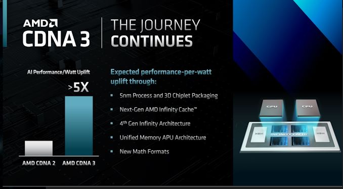
Alongside their Zen CPU architecture and RDNA client GPU architecture updates, AMD this afternoon is also updating their roadmap for their CDNA server GPU architecture and related Instinct products. And while CPUs and client GPUs are arguably on a rather straightforward path for the next two years, AMD intends to shake up its server GPU offerings in a big way.
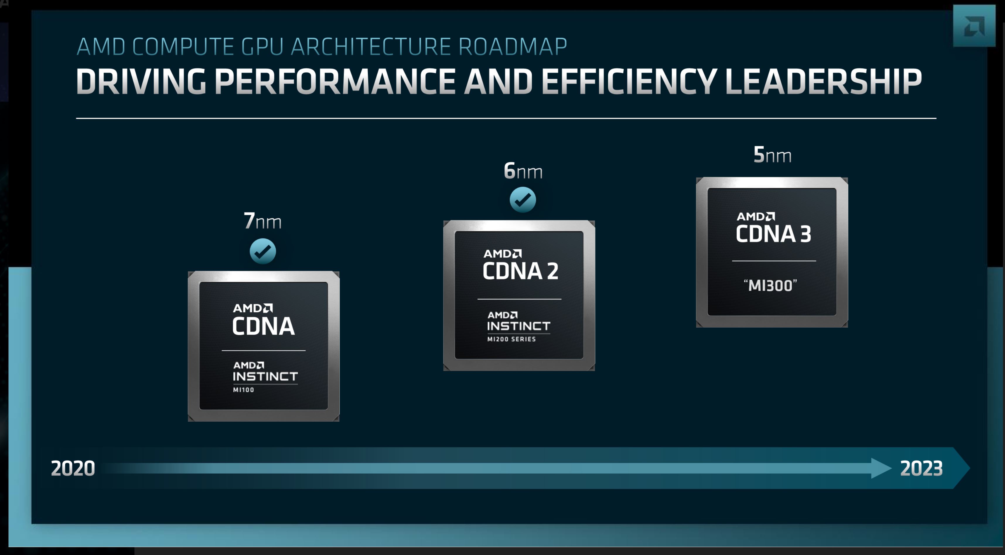
Let’s start first with AMD’s server GPU architectural roadmap. Following AMD’s current CDNA 2 architecture, which is being used in the MI200 series Instinct Accelerators, will be CDNA 3. And unlike AMD’s other roadmaps, the company isn’t offering a two-year view here. Instead, the server GPU roadmap only goes out one year – to 2023 – with AMD’s next server GPU architecture set to launch next year.
Our first look at CDNA 3 comes with quite a bit of detail. With a 2023 launch AMD isn’t holding back on information quite as much as they do elsewhere. As a result, they’re divulging information on everything from the architecture to some basic information about one of the products CDNA 3 will go in to – a data center APU made of CPU and GPU chiplets.
Taking things from the top, GPUs based on the CDNA 3 architecture will be built on a 5nm process. And like the CDNA 2-based MI200 accelerators before it, will rely on a chiplets to combine memory, cache, and processor cores all on a single package. Notably, AMD is calling this a “3D chiplet” design, which implies that not only are chiplets being stacked on to a substrate, but that some kind of chip is going to be stacked on top of other chiplets as well, ala AMD’s V-Cache for Zen 3 CPUs.
That comparison is particularly apt here as AMD is going to be introducing its Infinity Cache technology into the CDNA 3 architecture. And, like the V-Cache example above, judging from AMD’s artwork it appears that they are going to be stacking the cache with the logic as separate dies, rather than integrating it into a monolithic die like their client GPUs. Because of this stacked nature, the Infinity Cache chiplets for CDNA 3 will go below the processor chiplets, which AMD seemingly putting the very, very power-hungry logic chiplets at the top of the stack in order to effectively cool them.
CDNA 3 will also be employing AMD’s 4th generation Infinity Architecture. We’ll have more about that in a separate article, but the short version is that for GPUs, IA4 goes hand-in-hand with AMD’s chiplet innovations. Specifically, it will enable 2.5D/3D stacked chips to be used with IA, allowing for all of the chips within a package to share a unified and fully coherent memory subsystem. This is a big leap beyond IA3 and the current MI200 accelerators, which although offering memory coherency, doesn’t have a unified memory address space. So whereas MI200 accelerators function as essentially two GPUs on a single package, IA4 will let CDNA 3/MI300 accelerators to behave as a single chip, despite the disaggregated nature of the chiplets.
AMD’s diagrams also show HBM memory being once again used here. AMD does not specify what version of HBM, but given the 2023 timeframe it’s a very safe bet that it will be HBM3.
Architecturally, AMD will also be taking several steps to improve the AI performance of their high-performance accelerator. According to the company they are adding support for new mixed precision math formats. And while it’s not being explicitly stated today, AMD’s >5x improvement in performance-per-watt in AI workloads strongly implies that AMD is significantly reworking and expanding their matrix cores for CDNA 3, as 5x is well in excess of what fab improvements alone can deliver.
MI300: AMD’s First Disaggregated Data Center APU
But AMD isn’t stopping by just building a bigger GPU, nor are they unifying the memory pool for a multi-chiplet architecture merely to have GPUs working out of a shared memory pool. Instead, AMD’s ambitions are much greater than that. With high-performance CPU and GPU cores at their disposal, AMD is taking the next step in integration and is building a disaggregated, data center APU – a chip that combines CPU and GPU cores on to a single package.

The data center APU, which is currently codenamed MI300, is something AMD has been building to for a while now. With MI200 and Infinity Architecture 3 allowing AMD CPUs and GPUs to work together with a coherent memory architecture, the next step for a while has been to bring the CPU and GPU further together, both in terms of packaging and memory architecture.
For memory matters in particular, a unified architecture brings MI300 a couple major benefits. From a performance standpoint, this improves matters by eliminating redundant memory copies; processors no longer need to copy data over to their own dedicated memory pool to access/alter that data. The unified memory pool also means that there isn’t a second pool of memory chips required – in this case, the DRAM that would normally be attached to the CPU.
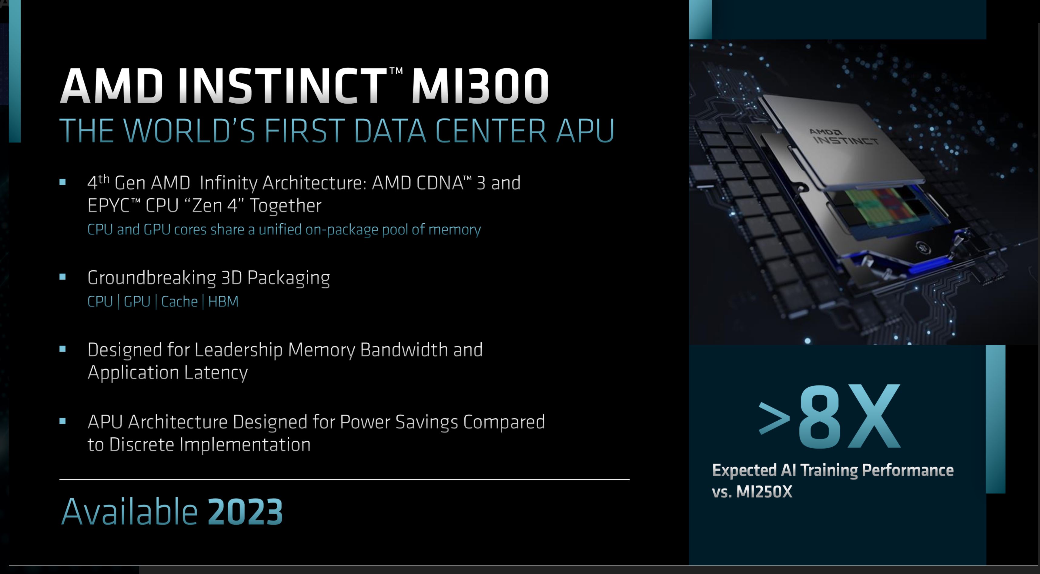
MI300 will combine CDNA 3 GPU chiplets and Zen 4 CPU chiplets on to a single processor package. Both of these processor pools, in turn, will share the on-package HBM memory. And, presumably, the Infinity Cache as well.
As previously mentioned, AMD is going to be heavily leveraging chiplets in order to accomplish this. The CPU cores, GPU cores, Infinity Cache, and HBM are all different chiplets, some of which will be stacked upon each other. So this will be chip unlike anything else AMD has built before, and it will be the most involved effort yet from AMD to integrate chiplets into their product designs.
Meanwhile, AMD is being very explicit about the fact that they’re gunning for market leadership in terms of memory bandwidth and application latency. Which if AMD can pull it off, would be a significant accomplishment for the company. With that said, they are not the first company to pair HBM with CPU cores – Intel’s Sapphire Rapids Xeon CPU will claim that accomplishment – so it will be interesting to see just how MI300 pans out in that regard.
As for the more specific matter of AI performance, AMD is claiming that the APU will offer better than 8x the training performance of the MI250X accelerator. Which is further evidence that AMD is going to be making some big enhancements to their GPU matrix cores versus the MI200 series.
Overall, AMD’s server GPU trajectory is fairly similar to what we’ve seen Intel and NVIDIA announce in the past several months. All three companies are building towards combined CPU+GPU products; NVIDIA with Grace Hopper (Grace + H100), Intel with Falcon Shores XPUs (mix & match CPU + GPU), and now MI300 with its use of both CPU and GPU chiplets on a single package. In all three cases, these technologies are aimed at combining the best of CPUs with the best of GPUs for workloads that are not purely bound by either – and in AMD’s case, the company believes they have the best CPUs and the best GPUs going into this process.
Expect to see a lot more on CDNA 3 and MI300 over the coming months.


16 Comments
View All Comments
ET - Saturday, June 11, 2022 - link
As a developer I'm in two minds about this. On one hand, there are times when using the CPU for specific parts of the code path can be helpful, and not having to transfer data for that will certainly help. On the other hand, one of the benefits of a discrete CPU is that it can have a large RAM space for relatively cheaply. Moving data to CPU RAM can help free GPU RAM. When GPU RAM is used for both CPU and GPU, there's less RAM for algorithms that need a lot of GPU data.Optimally I think it could be best to have the CPU and GPU share RAM but still have access to a large pool of slower, expandable RAM.
sgeocla - Saturday, June 11, 2022 - link
The MI300 has unified memory and with CXL.memory you can have access to as much memory as you want. That way you don't have to manage different CPU/GPU memory locations and just pass pointers around as you want. And with 3d v-cache the CPU and GPU can both have GB of local cache to access the HBM.mode_13h - Sunday, June 12, 2022 - link
It'll be interesting to see how well this scales to multiple APUs. The CPU cores embedded within a single APU will be a lot closer to those GPU dies, but not much closer to the GPU dies in another package than before. And if CPU <-> GPU communication now ends up getting routed through some other CPU cores, that could be a bit of a bottleneck.