Intel Rolls Out New Loihi 2 Neuromorphic Chip: Built on Early Intel 4 Process
by Dr. Ian Cutress on September 30, 2021 11:00 AM EST- Posted in
- CPUs
- Intel Labs
- Neuromorphic
- Intel 4
- Intel 4nm
- Loihi
- Loihi 2
- Neurons
- Synapses
We’ve been keeping light tabs on Intel’s Neuromorphic efforts ever since it launched its first dedicated 14nm silicon for Neuromorphic Computing, called Loihi, back in early 2018. In an interview with Intel Lab’s Director Dr. Richard Uhlig back in March 2021, I asked about the development of the hardware, and when we might see a second generation. Today is that day, and the group is announcing Loihi 2, a substantial upgrade over the first generation that addresses a lot of the low-hanging fruit from the first design. What is perhaps just as interesting is the process node used: Intel is communicating that Loihi 2 is being built, in silicon today, using a pre-production version of Intel’s first EUV process node, Intel 4.
Neuromorphic Computing for Intel
By creating an architecture that at its core is modeled like a brain, the idea is that having millions of neurons and synapses will lead to compute tasks with the unique power/performance benefits in specific tasks that brains are designed to do. It’s a long term potential commercial product for Intel, however the task for the team has been to develop both the technology and the software to discover and accelerate tasks that are suited to neuron-type computing.

The Neuromorphic Lab at Intel was actually borne out an acquisition of Fulcrum Microsystems in 2011. At the time, the Fulcrum team was an asynchronous computing group working on network switches. That technology was moved up to the networking group inside Intel, and the research division turned its attention to other uses of asynchronous compute, and landed on Neuromorphic.
At that time, research into this sort of neuromorphic computing architecture for actual workloads was fairly nascent – while the field wad been around since the late 1980s, dedicated research-built hardware didn’t really exist until the early 2010s. The Human Brain Project, a 10 year research project funded by the European Union to look into this field, was only established in 2013, and out of that is the SpiNNaker system in 2019, with a million chips, a billion neurons, for 100 kW of active power.
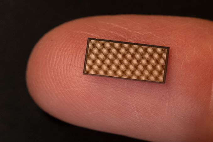
By comparison Intel’s first generation Loihi supports 131000 neurons per 60 mm2 chip, and 768 chips can be put together in a single Pohoiki Springs system with 100 million neurons for only 300 watts. In Intel’s own marketing, they’ve described this as the equivalent to a hamster. The new Loihi 2 chip, at a high level, uses 31 mm2 per chip for a million neurons, effectively increasing density 15x, however the development goes beyond raw numbers.
Loihi 2
The Loihi 2 chip at a high level might look similar: 128 neuromorphic cores, but now each core has 8x more neurons and synapses. Each of those 128 cores has 192 KB of flexible memory, compared to previously where it was fixed per core at runtime, and each neuron can be allocated up to 4096 states depending on the model, whereas the previous limit was only 24. The Neuron model can also now be fully programmable, akin to an FPGA, allowing for greater flexibility.

Traditionally neurons and spiked networks deliver data in a binary event, which is what Loihi v1 did. With Loihi 2, those events can be graded with a 32-bit payload, offering deeper flexibility for on-chip compute. Those events can now be monitored in real time with new development/debug features on chip, rather than pause/read/play. In combination, this also allows for better control when dynamically changing compute workloads, such as fan-out compression, weight scaling, convolutions, and broadcasts.
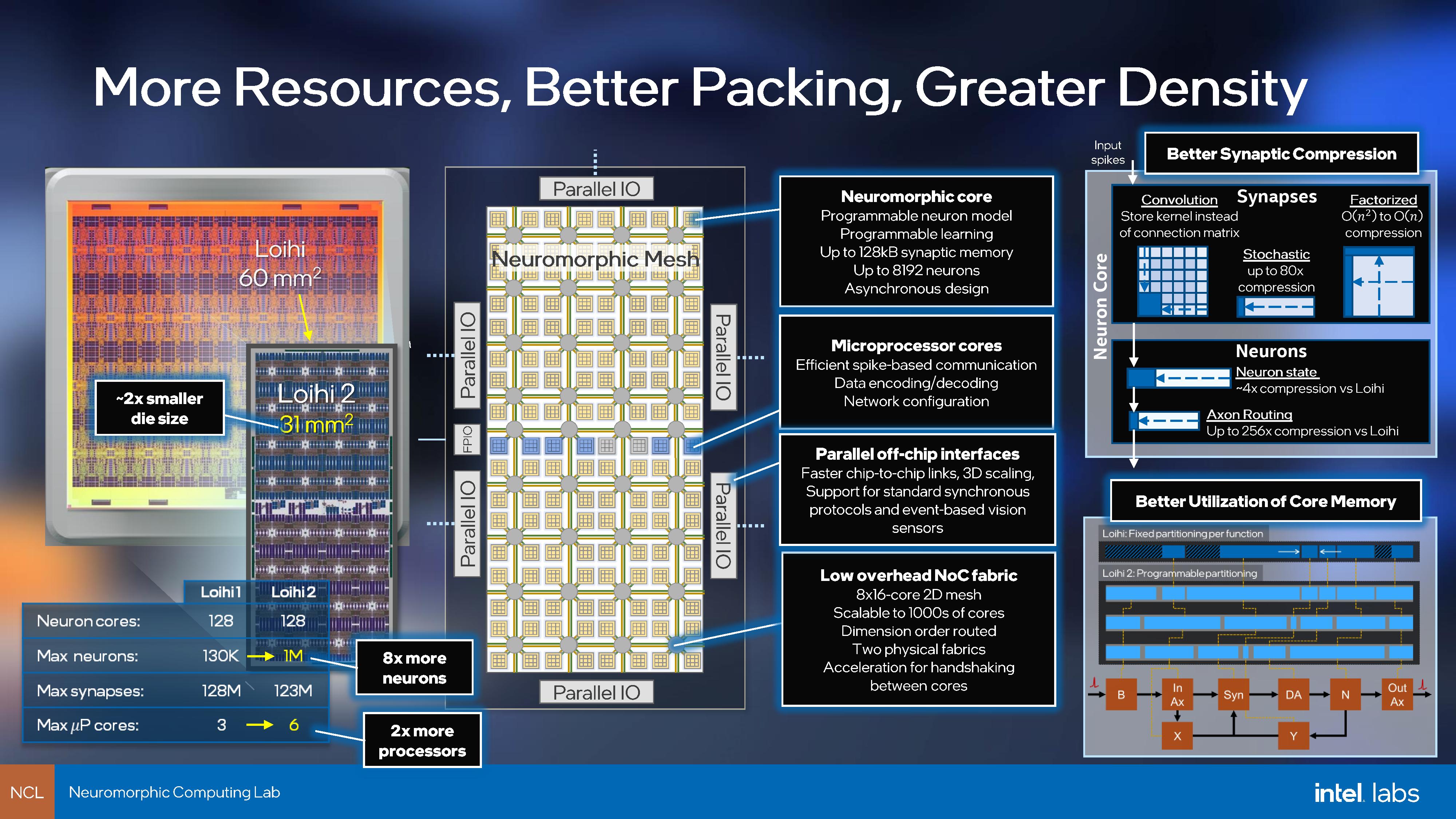
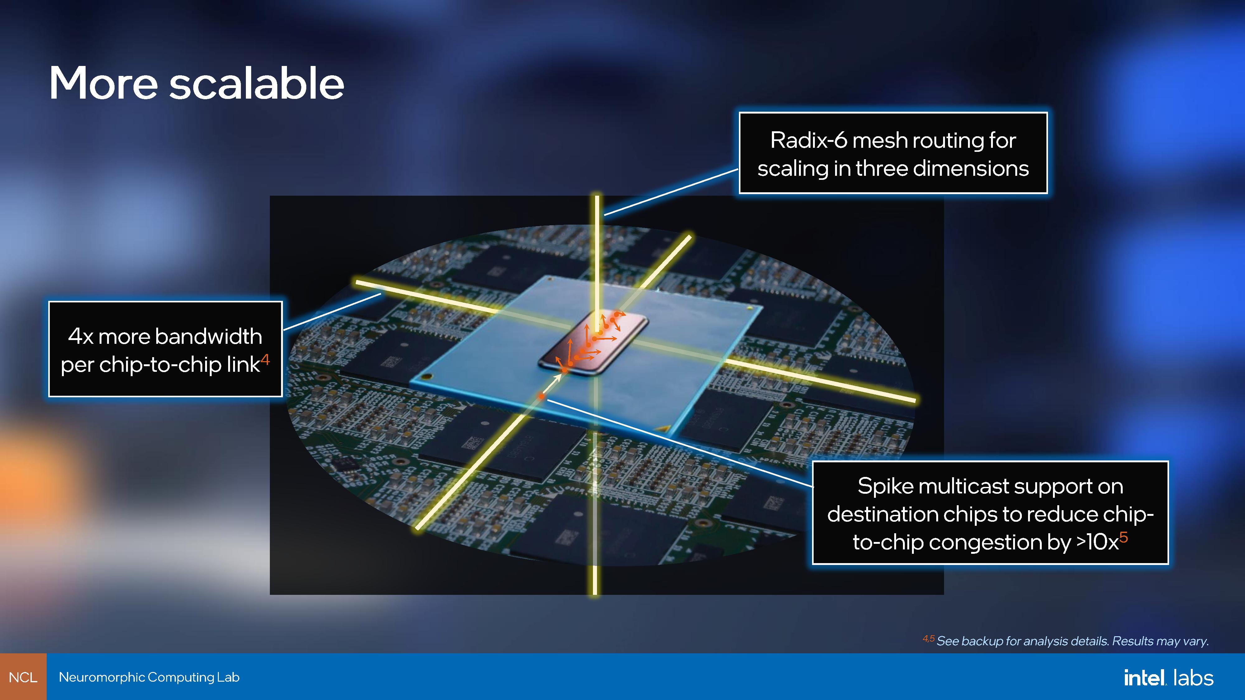
Perhaps one of the biggest improvements is in connectivity. The first generation used a custom asynchronous protocol to create a large 2D network of neurons, while Loihi 2 can be configured to use a variety of protocols based on need, but also in a 3D network. We were told that Loihi 2 isn’t just a single chip, but it will be a family of chips with the same neuron architecture but a variety of different connectivity options based on specific use cases. This can be used in conjunction with onboard message compression accelerators to get an effective 10x increase in chip-to-chip bandwidth.
This also extends to external Loihi connectivity to more conventional computing, which was previously FPGA mediated – now Loihi 2 supports 10G Ethernet, GPIO, and SPI. This should allow for easier integration without the need for custom systems, such as creating disaggregated Loihi 2 compute clusters.
Built on Intel 4
We were surprised to hear that Loihi 2 is built on a pre-production version of Intel 4 process. We are still a time away from Loihi 2 being a portion of Intel’s revenue, and the Neuromorphic team knows as much, but it turns out that the chip is perhaps an ideal candidate to help bring up a new process.
At 31 mm2, the size means that even if the yield needs to improve, a single wafer can offer more working chips than testing with a bigger die size. As the team does post-silicon testing for voltage/frequency/functionality, they can cycle back quicker to Intel’s Technology Development team. We confirmed that there is actual silicon in the lab, and in fact the hardware will be available today through Intel’s DevCloud, direct to metal, without any emulation.
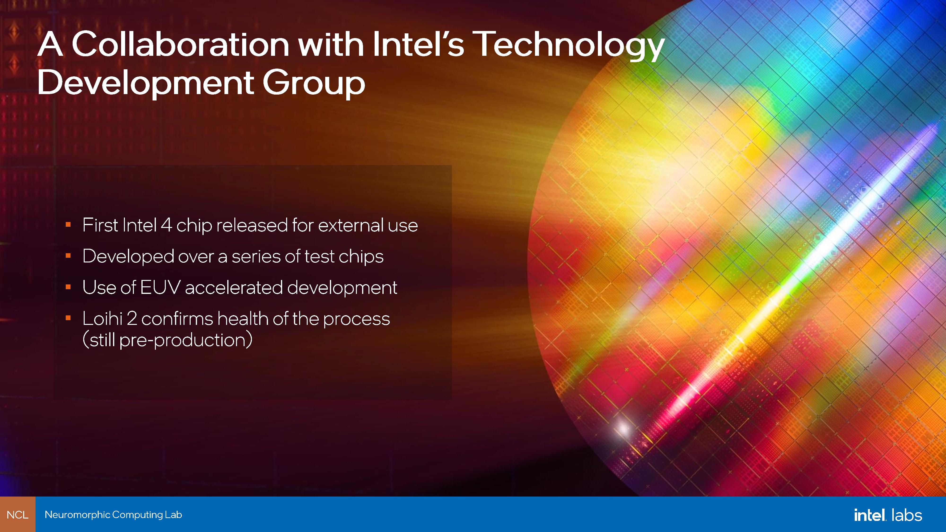
Normally with new process nodes, you need a customer with a small silicon die size to help iterate through the potential roadblocks in bringing a process up to a full-scale ramp and production. Intel’s foundry competitors normally do this with customers that have smartphone-sized chips, and the benefits for the customer usually means first to hardware or perhaps some sort of initial discount (although, perhaps not in today’s climate). Intel has previously struggled on that front, as it only has its own silicon to use as a test vehicle.
The Neuromorphic team said that it was actually a good fit, given that neuromorphic hardware requires the high density and low static power afforded by the leading edge process nodes. The 128-core design also means that it has a consistent repeating unit, allowing the process team to look at regularity and consistency in production. Also, given that Loihi still remains a research project for now, there’s no serious expectation to drive that product to market in a given window, which perhaps a big customer might need.
Does this mean Intel’s 4 is ready for production? Not quite, but it does indicate that progress is being made. A number of Loihi 2’s listed benchmarks did have the caveat of ‘expected given simulated hardware results’, although a few others were done on real silicon, and the company says it has real silicon to deploy in the cloud today. Intel 4 is Intel’s first process node that Extreme Ultra Violet (EUV) lithography, and Intel will be the last major semi manufacturer to initiate an EUV process for productization. But we’re still a way off – back at Intel’s Accelerated event, EUV and Intel 4 isn’t really isn’t expected to ramp production until the second half of 2022.
To wrap up, from Intel’s announcement, we are able to look at transistor density. At 2.3 billion transistors in 31 mm2, that would put the density at 71.2 million per mm2, which is only a third of what we are expecting. Estimates based on Intel’s previous announcements would put Intel 4 at around 200 MTr/mm2. So why is Loihi 2 so low compared to that number?
First is perhaps that it is a neuromorphic chip, and not a traditional logic design. The core has ~25 MB of SRAM total along with all the logic, which for a 31mm2 chip might be a good chunk of the die area. Also, Intel’s main idea with the neuromorphic chips is functionality first, performance second, and power third. So getting it working right is more important than getting it working fast, so there isn’t always a raw need for the highest density. Then there’s the fact that it’s still a development chip, and it allows Intel to refine its EUV process and test for precision lithography without having to worry as much about defects caused by dense transistor libraries. More to come, I’m sure.
To add a final point, our briefing did speculate that the neuromorphic IP could potentially be made available through Intel’s Foundry Service IP offerings in the future.
New Lava Software Framework
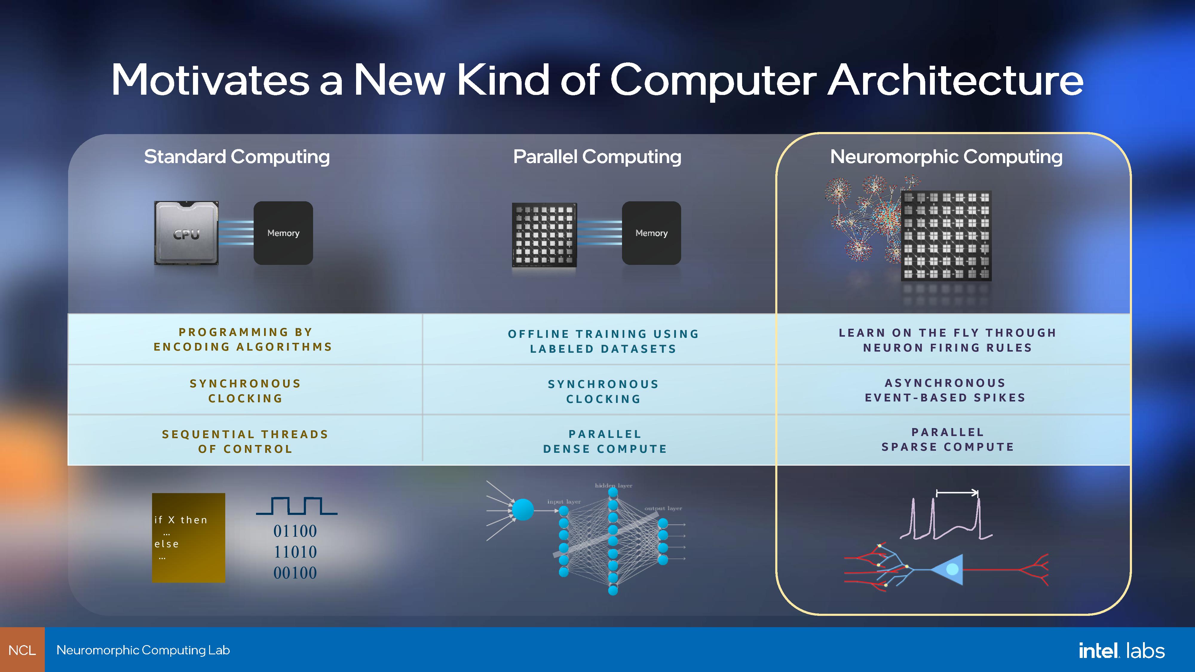
Regardless of processing capability, one of the main building blocks for a Neuromorphic system is the type of compute, and perhaps how difficult it is to write software to take advantage of such an architecture. In a discussion with Intel’s Mike Davies, Director of Intel’s Neuromorphic Lab, we best described it that modern computing is akin to a polling architecture – every cycle it takes data and processes it. By contrast, Neuromorphic computing is an interrupt based architecture – it acts when data is ready. Neuromorphic computing is moreso time domain dependent than modern computing, and so both the concept of compute and the applications it can work on are almost orthogonal to traditional computing techniques. For example, while machine learning can be applied to neuromorphic computing in the form of Spiking Neural Networks (SNNs), traditional PyTorch and TensorFlow libraries aren’t built to enable SNNs.
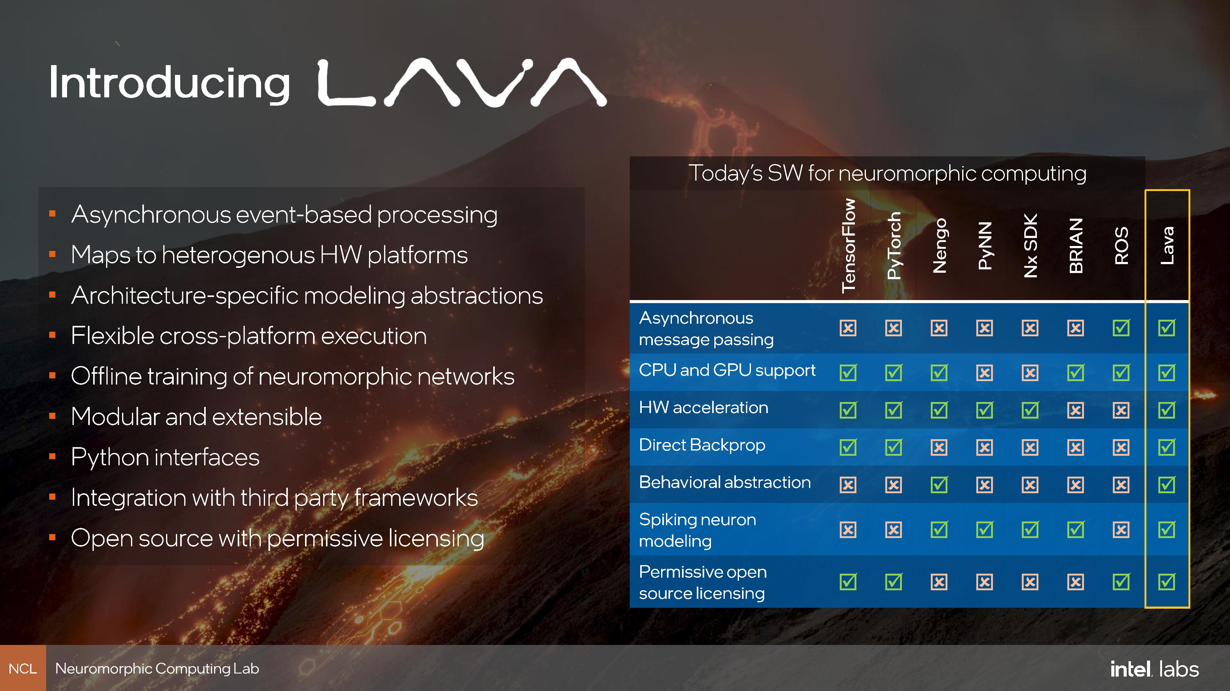
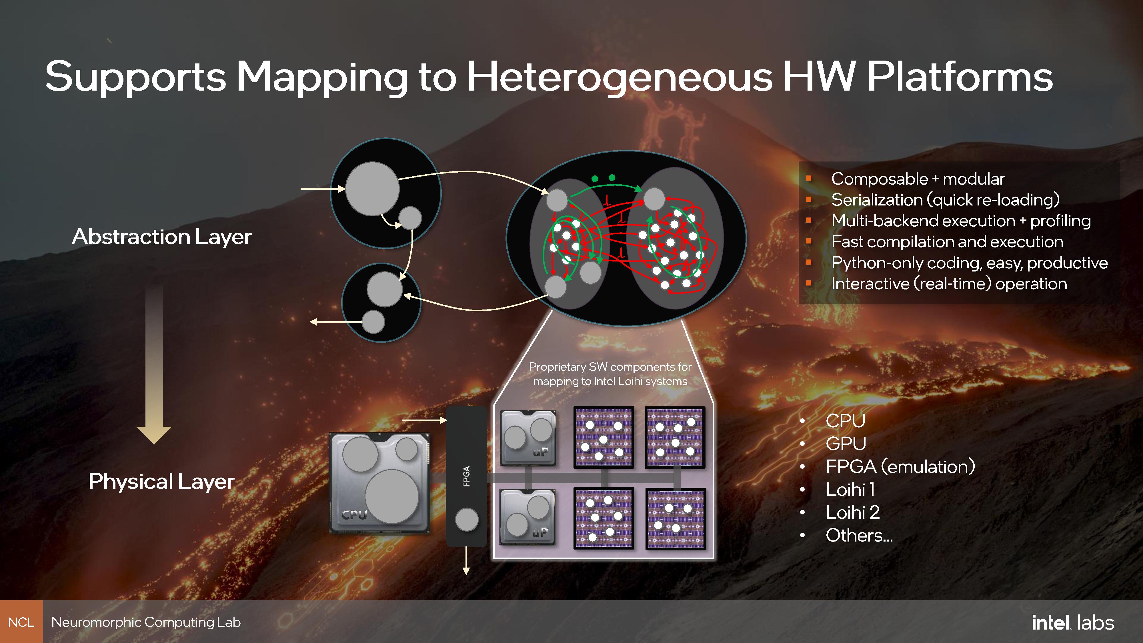
Today, as part of the announcements, Intel is launching a new underlying software framework for the neuromorphic community called Lava. This is an open source framework, not under Intel’s control, but by the community. Intel has pushed a number of its early tools as part of the framework, and the idea is that over time a full software stack can be developed for everyone involved in Neuromorphic computing to use, regardless of the hardware (CPU, GPU, Neuromorphic chip). Lava is designed to be modular, composable, extensible, hierarchical, and open-source. This includes a low-level interface for mapping neural networks onto neuromorphic hardware, channel-based asynchronous message passing, and all libraries and features are exposed through Python. The software will be available for free use under BSD-3 and LGPL-2.1 at GitHub.
Initial Systems
The first version of Loihi 2 to deployed in Intel’s cloud services is Oheo Gulch, which looks like a PCIe add-in card using an FPGA to manage a lot of the IO, along with a backplane connector if needed. The 31 mm2 chip is BGA, and here we’re seeing one of Intel’s internal connectors for holding BGA chips onto a development board.

At a future date, Intel will produce a 4-inch by 4-inch version called Kapoho Point, with eight chips on board, designed to be stacked and integrated into a larger machine.
With having such a small chip, I wonder if it’s not worthwhile building it with a USB controller on the silicon, or having a USB-to-Ethernet interface, and offering the hardware on USB sticks, akin to what Intel’s Movidius used to be distributed. We asked Intel about expanding the use of Loihi 2 out to a wider non-research/non-commercial focused audience to tinker and homebrew, however as this is still an Intel Labs project right now, one of the key elements for the team is the dedicated collaborations they have with partners to push the segment forward. So we’re going to have to wait at least another generation or more to see if any future Loihi systems end up being offered on Amazon.
Loihi 2 should be availble for research partners to use from today as part of Intel's DevCloud. On-premises research/collaboration deployments are expected over the next 12-24 months.
Related Reading
- The Intel Moonshot Division: An Interview with Dr. Richard Uhlig of Intel Labs
- Intel at CES 2018 Keynote Live Blog


68 Comments
View All Comments
m53 - Thursday, September 30, 2021 - link
Your concern was "When you tell a lie over and over again people will actually think it is 4nm when it isn't". Yet you were fine letting TSMC lie when calling their N5 process as 5nm. There isn't any 5nm feature in TSMC N5.Now regarding Intel's official naming, this is NOT an Intel official site. It's Anandtech. They are not required to follow intel's marketing guidelines. He just has to do a fair review of the process and make it easy to understand for the reader. In his previous article, Ian already explained how Intel 7 is similar to TSMC N7 and how Intel 3 is expected to be similar to future TSMC N3. Hence calling Intel 4 process 4nm makes it easier for the general reader to understand where the performance stands.
shabby - Friday, October 1, 2021 - link
Good news... Ian changed it so no need so use reverse psychology on me.catavalon21 - Thursday, September 30, 2021 - link
My point was his prior entire article is how the naming convention is leaving "dimensions" behind - nanometers, angstroms, whatever. Just a number. And yes, the effort put into pointing all that out could have been spend doing far better things.Spunjji - Friday, October 1, 2021 - link
"It also helps laymen’s to understand this this node is slightly better performing than TSMC N5 (commonly known as 5nm)."We don't yet know this, though. All we know is that's where Intel expect it to land. They told us 10nm would be around 50% more dense than TSMC N7, and it isn't.
Lakados - Monday, October 4, 2021 - link
We already know that Intel's 7nm process is roughly equivalent to the TSMC 5 as Intel has been using TSMC's 5 to cover their own 7nm shortfall with the Aurora supercomputer. From internal reports, the Intel 7nm (now Intel 4) performed nearly identically with the TSMC produced chips to the degree where the only discernable difference was the SKU numbers on the card that identified them as different.eastcoast_pete - Thursday, September 30, 2021 - link
Regardless of what size the structures really are, I took two things away from this article: 1. These neuromorphic processors are cool tech, something to watch, and 2. Intel is seriously gearing up for EUV in their manufacturing. Point 2 is good news for all of us, because I fully expect AMD moving its next generation to TSMC's 5 nm or better to keep up. Interestingly, that leaves NVIDIA bringing up the rear in what node they are on. Samsung 8 is far from either TSMC 7 or Intel 7.Spunjji - Friday, October 1, 2021 - link
Last I'd heard, Nvidia were considering moving back to TSMC. Still, if they go with Samsung 5nm for their next products, they'll get something close to TSMC N7 in electrical performance but with higher density (and less competition for wafers). That might work reasonably well for them given the generally high energy efficiency of their architectures.wrkingclass_hero - Friday, October 1, 2021 - link
Thank you Ian for clearing up the title.Spunjji - Friday, October 1, 2021 - link
I found this very interesting, both in terms of being a novel area of computing I'm not familiar with and to see what Intel have chosen as a "pipecleaner" for their next gen process. It's certainly a more interesting project than printing out little dual-core CPU dies!Cheers for the good content, Ian.
Diogene7 - Friday, October 1, 2021 - link
@Ian: I was wondering if there would be any chance to get an article that would compare the new Intel Loihi 2 chip versus IBM Synpase Truenorth chip, because I think both are roughly 1 million neurons chip ?What are the architectural differences and what each of them can / can’t do ?
I would be very curious to know…