Intel Architecture Day 2021: Alder Lake, Golden Cove, and Gracemont Detailed
by Dr. Ian Cutress & Andrei Frumusanu on August 19, 2021 9:00 AM EST
This week Intel held its annual Architecture Day event for select press and partners. As with previous iterations, the company disclosed details about its next generation architectures set to come to the market over the next twelve months. Intel has promised the release of its next-generation consumer and mobile processor family, Alder Lake, to come by the end of the year and today the company is sharing a good number of details about the holistic design of the chips as well as some good detail about the microarchitectures that form this hybrid design: Golden Cove and Gracemont. Here is our analysis of Intel’s disclosure.
Alder Lake: Intel 12th Gen Core
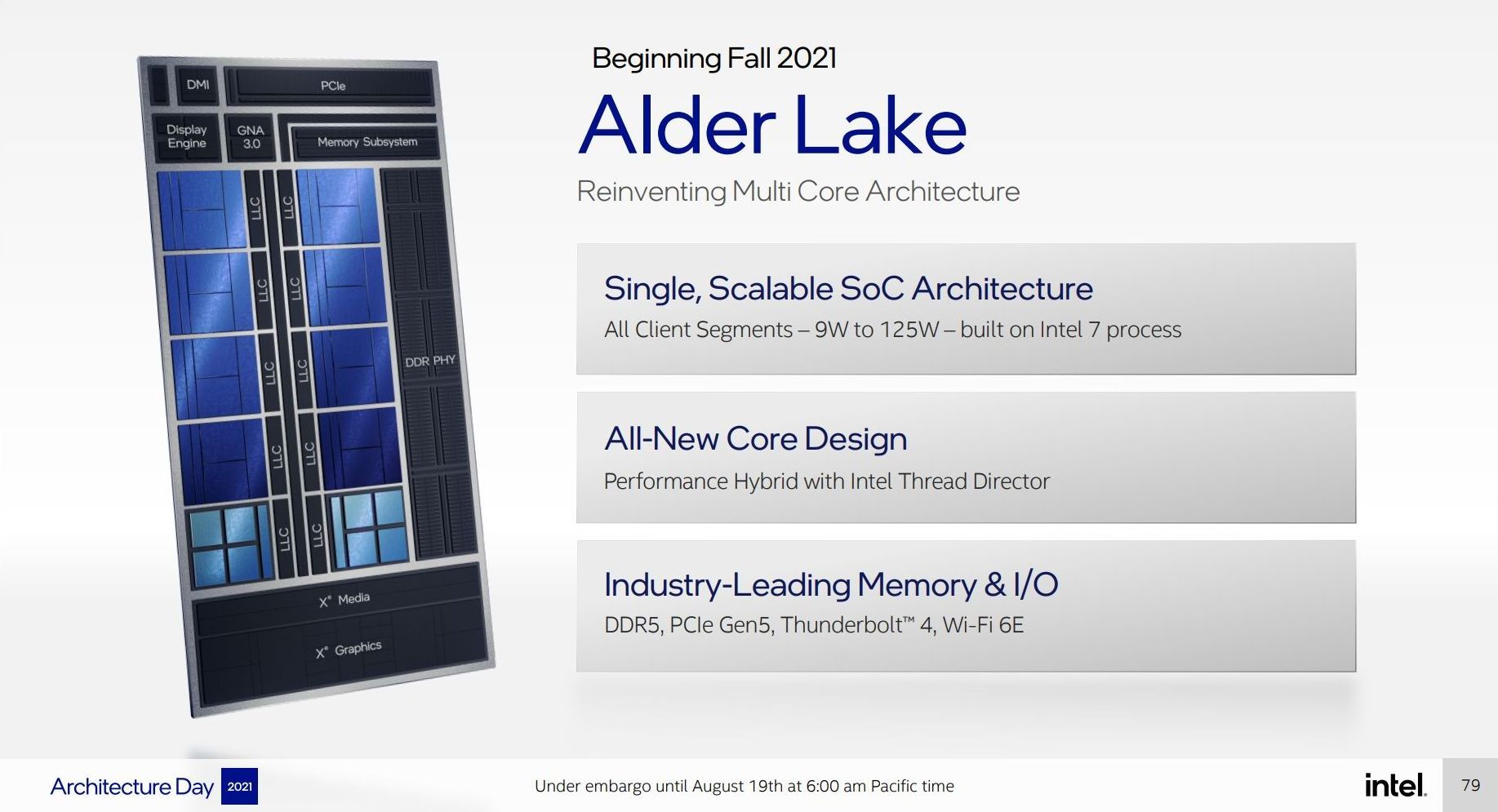
As mentioned in previous announcements, Intel will launch its Alder Lake family of processors into both desktop and mobile platforms under the name of Intel’s 12th Gen Core Processors with Hybrid Technology later this year. This is Intel’s second generation hybrid architecture built on Intel 7 process node technology. The hybrid design follows Intel Lakefield designs for small notebooks launched last year. The nature of a hybrid design in Intel nomenclature involves having a series of high ‘Performance’ cores paired with a number of high ‘Efficiency’ cores. Intel has simplified this into P-core and E-core terminology.
For Alder Lake, the processor designs feature Performance cores based on a new Golden Cove microarchitecture, and Efficiency cores based on a new Gracemont architecture. We will cover both over the course of this article, however the idea is that the P-core is preferential for single threaded tasks that require low latency, and the E-core is better in power limited or multi-threaded scenarios. Each Alder Lake SoC will physically contain both, however Intel has not yet disclosed the end-user product configurations.
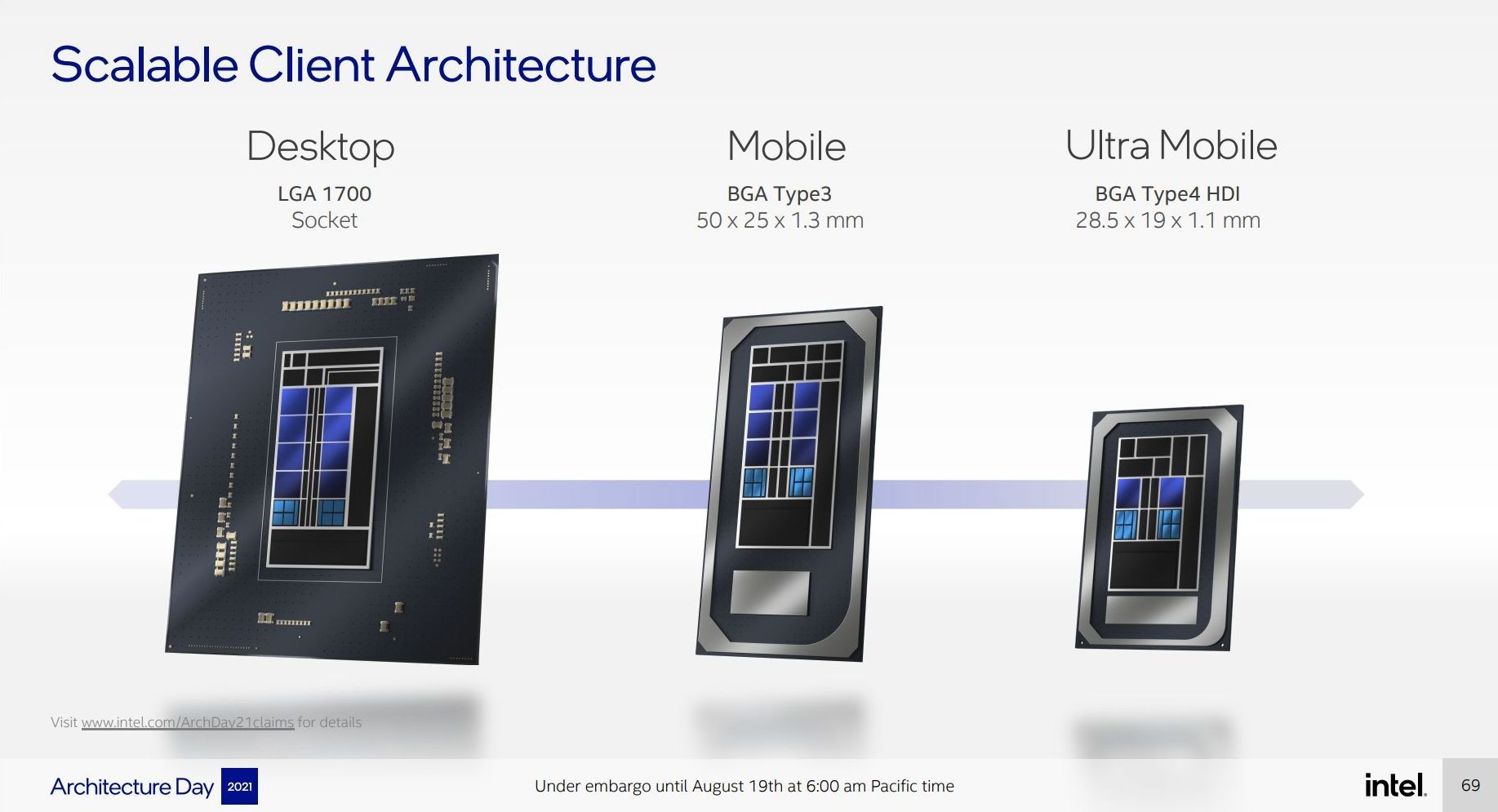
Each of the P-cores has the potential to offer multithreading, whereas the E-cores are one thread per core. This means there will be three physical designs based on Alder Lake:
- 8 P-core + 8 E-core (8C8c/24T) for desktop on a new LGA1700 socket
- 6 P-core + 8 E-core (6C8c/20T) for mobile UP3 designs
- 2 P-core + 8 E-core (2C8c/12T) for mobile UP4 designs
Intel typically highlights UP4 mobile designs for very low power installs, down to 9 W, whereas UP3 can cover anything from 12 W to 35 W (or perhaps higher), but when asked about the power budgets for these processors, Intel stated that more detail will follow when product announcements are made. Intel did confirm that the highest client power, presumably on the desktop processor, will be 125 W.
Highlighted in our discussions is how modular Intel has made Alder Lake. From a range of base component options, the company mixed and matched what it felt were the best combination of parts for each market.
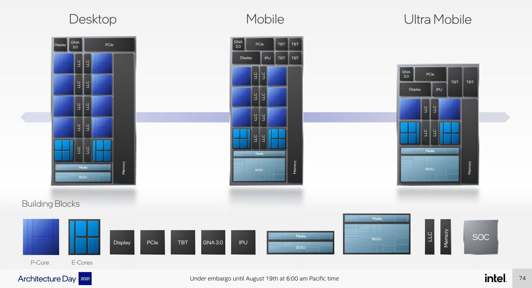
Here it shows that four E-cores takes up the same physical space as one P-core, but also that the desktop hardware will at most have 32 EUs (Execution Units) for Xe-LP graphics (same as the previous generation), while both of the mobile processors will offer 96 physical EUs that may be disabled down based on the specific line item in the product stack.
All three processors will feature Intel’s next generation Gaussian Neural Accelerator (GNA 3.0) for minor low power AI tasks, a display engine, and some level of PCIe, however the desktop processor will have more. Only the mobile processors will get an Image Processing Unit (IPU), and Thunderbolt 4 (TBT), and here the big UP3 mobile processor gets four ports of Thunderbolt whereas the smaller UP4 will only get two. The desktop processor will not have any native Thunderbolt connectivity.
A bit more info on the Desktop Processor IO and Interconnect
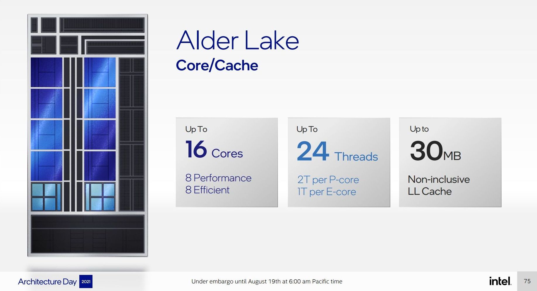
We’ll cover a bit more detail about the core designs later in this article, but Intel did showcase some of the information on the desktop processor. It confirmed explicitly that there would be 16 total cores and 24 threads, with up to 30 MB of non-inclusive last level/L3 cache.
In contrast to previous iterations of Intel’s processors, the desktop processor will support all modern standards: DDR5 at 4800 MT/s, DDR4-3200, LPDDR5-5200, and LPDDR4X-4266. Alongside this the processor will enable dynamic voltage-frequency scaling (aka turbo) and offer enhanced overclocking support. What exactly that last element means we’re unclear of at this point.
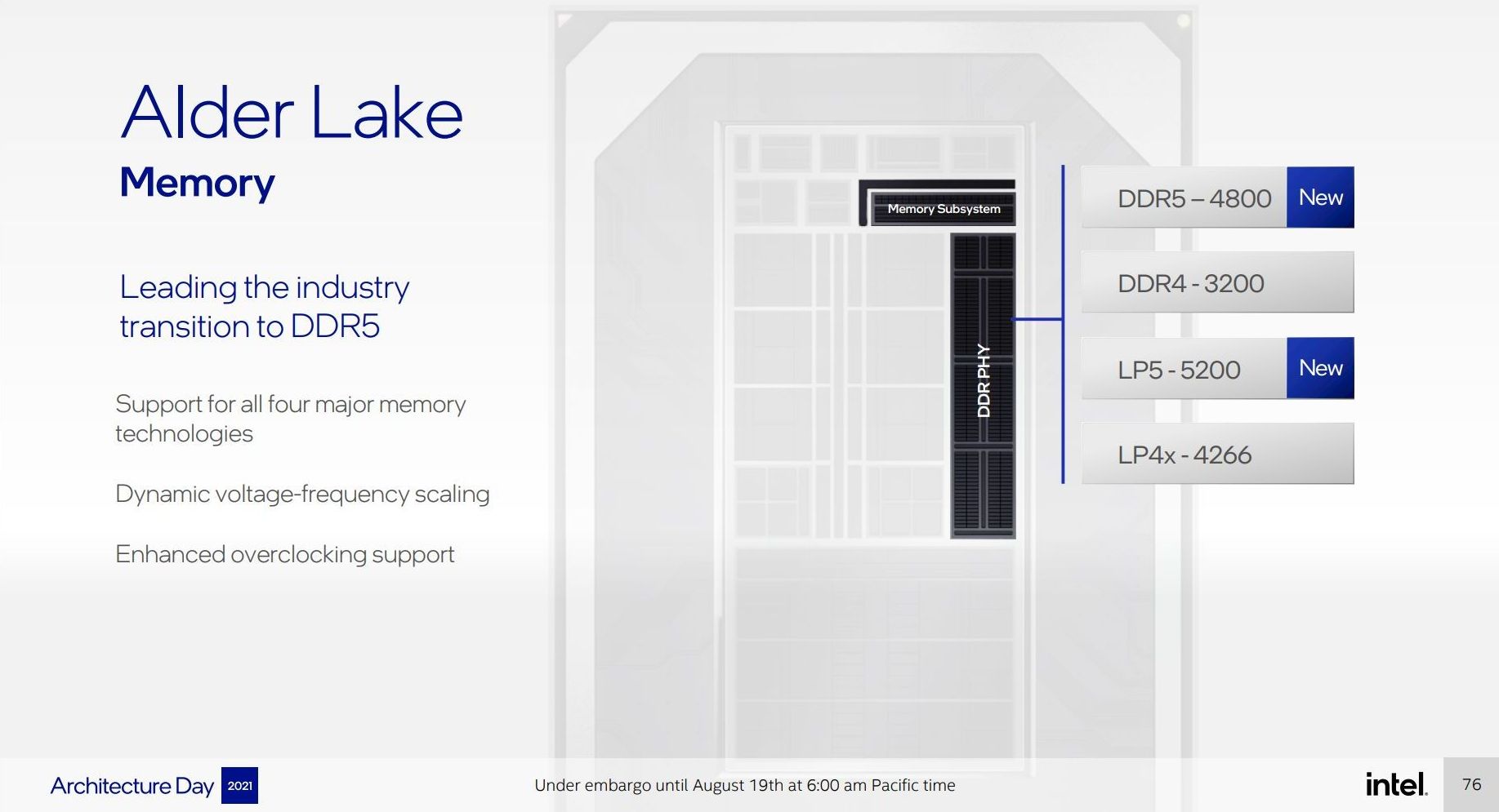
Intel confirmed that there will not be separate core designs with different memory support – all desktop processors will have a memory controller that can do all four standards. What this means is that we may see motherboards with built-in LPDDR5 or LPDDR4X rather than memory slots if a vendor wants to use LP memory, mostly likely in integrated small form factor designs but I wouldn’t put it past someone like ASRock to offer a mini-ITX board with built in LPDDR5. It was not disclosed what memory architectures the mobile processors will support, although we do expect almost identical support.
On the PCIe side of things, Alder Lake’s desktop processor will be supporting 20 lanes of PCIe, and this is split between PCIe 4.0 and PCIe 5.0.
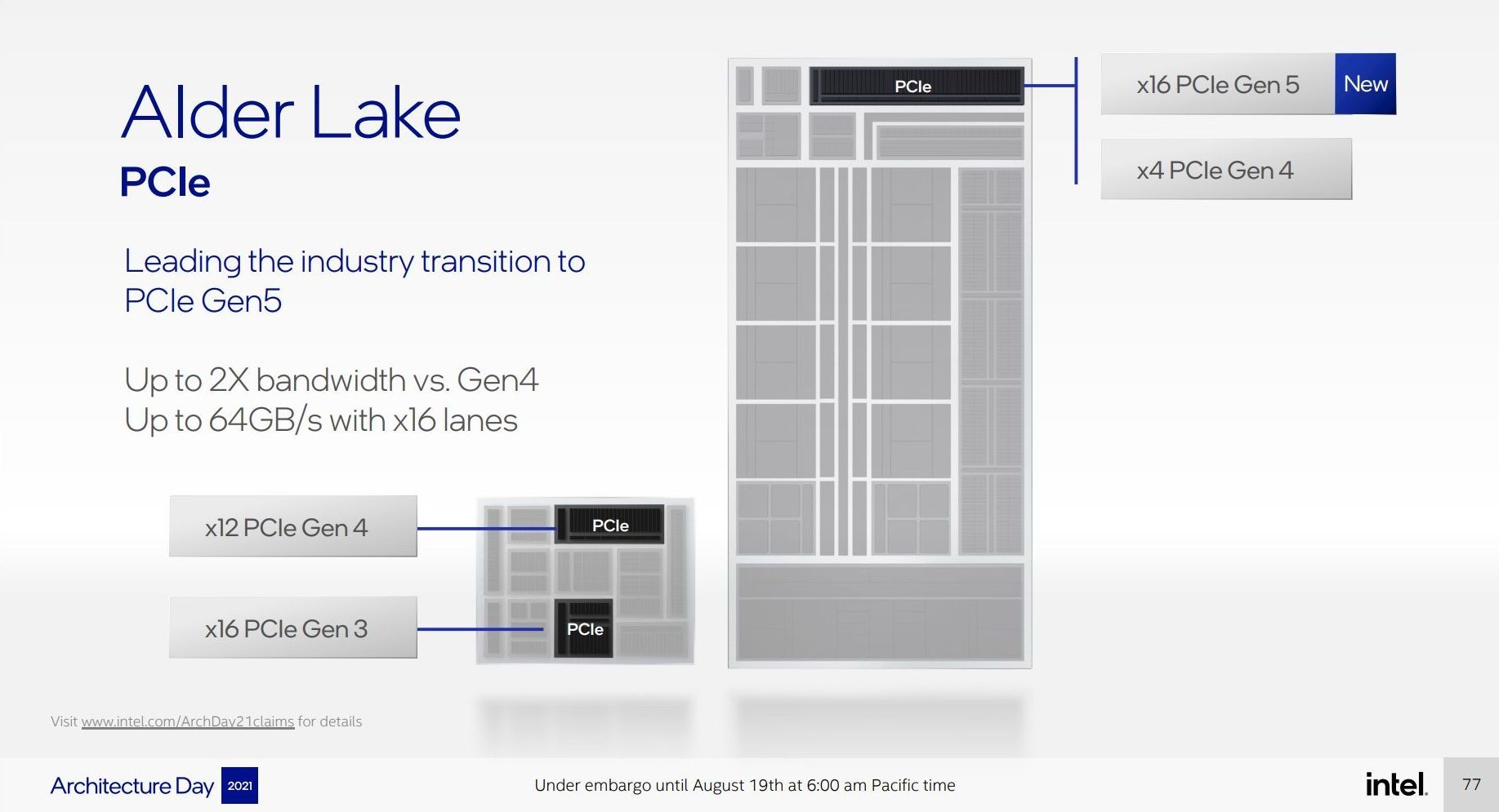
The desktop processor will have sixteen lanes of PCIe 5.0, which we expect to be split as x16 for graphics or as x8 for graphics and x4/x4 for storage. This will enable a full 64 GB/s bandwidth. Above and beyond this are another four PCIe 4.0 lanes for more storage. As PCIe 5.0 NVMe drives come to market, users may have to decide if they want the full PCIe 5.0 to the discrete graphics card or not
Intel also let it be known that the top chipset for Alder Lake on desktop now supports 12 lanes of PCIe 4.0 and 16 lanes of PCIe 3.0. This will allow for additional PCIe 4.0 devices to use the chipset, reducing the number of lanes needed for items like 10 gigabit Ethernet controllers or anything a bit spicier. If you ever thought your RGB controller could use more bandwidth, Intel is only happy to provide.
Intel did not disclose the bandwidth connectivity between the CPU and the chipset, though we believe this to be at least PCIe 4.0 x4 equivalent, if not higher.
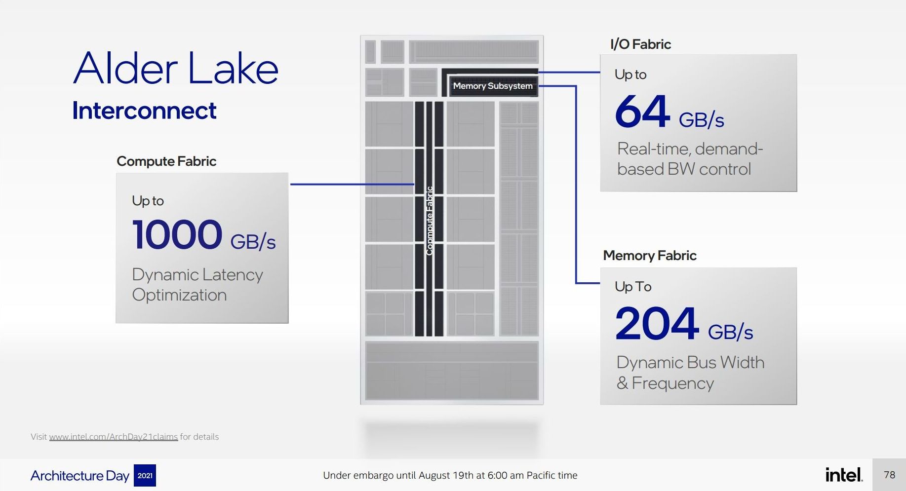
The Alder Lake processor retains the dual-bandwidth ring we saw implemented in Tiger Lake, enabling 1000 GB/s of bandwidth. We learned from asking Intel in our Q&A that this ring is fully enabled regardless of whether the P-cores or E-cores are being used – Intel can disable one of the two rings when less bandwidth is needed, which would save power, however based on previous testing this single ring could end up drawing substantial power compared to the E-cores in low power operation. (This may be true in the mobile processors as well, which would have knock on effects for mobile battery life.)
The 64 GB/s of IO fabric is in line with the PCIe 5.0 x16 numbers we saw above, however the 204 GB/s of memory fabric bandwidth is a confusing number. Alder Lake features a 128-bit memory bus, which allows for 4x 32-bit DDR5 channels (DDR5 has two 32-bit channels per module, so 2 modules still), however in order to reach 204 GB/s in that configuration requires DDR5-12750; Intel has rated the processor only at DDR5-4800, less than half that, so it is unclear where this 204 GB/s number comes from. For perspective, Intel’s Ice Lake does 204.8 GB/s, and that’s a high-power server platform with 8 channels of DDR4-3200.
This final slide mentions TB4 and Wi-Fi 6E, however as with previous desktop processors, these are derived from controllers attached to the chipset, and not in the silicon itself. The mobile processors will have TBT integrated, but the desktop processor does not.
This slide also mentions Intel Thread Director, which we want to address on the next page before we get to the microarchitecture analysis.


223 Comments
View All Comments
mode_13h - Friday, August 20, 2021 - link
> they can't exactly prevent open source software from developingWell, they don't have to release all of the information that would be needed for Linux to do the same thing.
> Linux will probably have better support than Windows itself
Intel is one of the largest contributors to the Linux kernel. No doubt, any support for their Thread Director will be developed by them.
Obi-Wan_ - Thursday, August 19, 2021 - link
Is it likely that Alder Lake will consume noticeably less power when near idle or during video playback/streaming, or are existing CPUs already quite efficient in these cases?I'm thinking an HTPC that should be as silent as possible when idling and streaming, but also have a high power budget (effectively noise budget) when gaming for example.
mode_13h - Friday, August 20, 2021 - link
If you really care about minimizing idle power, then I think you probably need to use LPDDR memory. Integrated graphics should also be a priority.Another thing people miss is that the PSU should not only be a high-efficiency model, but also not heavily over-spec'd. Power supplies lose a lot of efficiency, when you run them well below peak load.
mode_13h - Thursday, August 19, 2021 - link
> The desktop processor will have sixteen lanes of PCIe 5.0I'll believe it when I see it. Let's not forget that it took Intel 2 generations to get PCIe 4.0 working! They had to reverse course on enabling it it Comet Lake, and that was years after POWER, Ryzen, and some ARM CPUs had it.
I also don't see the value of having it now, given that we know DG2 is going to be only PCIe 4, nor are we aware of any other upcoming GPUs that will support 5.0.
Bp_968 - Sunday, August 22, 2021 - link
Pcie 5 is twice as fast and backwards compatible. Why would you *not* want it in your system if possible? Its not like you can add it later.Pcie4 is mostly useless for gpus already (regardless if they "support" it or not) so pcie5 isnt going to improve anything gpu wise just like it didnt improve with pcie4.
But where it *will* be an improvement is in peripherals (the x4 channel to the chipset just got twice as fast) and support for pcie5 storage. Oh and easier support for high speed interconnects like USB 3-4 and 10gb ethernet.
Personally id prefer the layout be different. X16 or X8/x8 (plus 2 x4 slots for nvme i think) for the pcie5 is ok, but on the pcie4 side I'd like to see x16, x8/x8 as an option as well. That way you could use the pcie5 slots on other stuff and put the gpu in a x16 or x8 pcie4 slot (and it perform just as well). Support for 4+ nvme drives will be nice in the future. One or two pcie5 high speed units and then spots for slower SSDs for mass storage (x2 or x4 pcie4 being the "slow" slots).
mode_13h - Monday, August 23, 2021 - link
> Pcie 5 is twice as fast and backwards compatible.> Why would you *not* want it in your system if possible?
Mainly due to board and peripheral costs, I think. Beyond that, power dissipation should be well above PCIe 4.0 and it could also be a source of stability issues.
> But where it *will* be an improvement is in peripherals
> (the x4 channel to the chipset just got twice as fast)
This is actually the one place where it makes sense to me. The chipset can be located next to the CPU, so that hopefully no retimers will be needed. And the additional power needed to run a short x4 link @ 5.0 speeds hopefully shouldn't be too bad. When leaks first emerged about Alder Lake having PCIe 5.0, I suspected it was just for the chipset link.
> support for pcie5 storage.
By the time there are any consumer SSDs that exceed PCIe 4.0 x4 speeds, we'll already be on a new platform. It took over a year for PCIe 4.0 SSDs to finally surpass PCIe 3.0 x4 speeds, and many still don't.
> easier support for high speed interconnects like USB 3-4
The highest-rated speed for USB4 is PCIe 3.0 x4. However, even a chipset link of PCIe 4.0 x4 will mean you can support it with bandwidth to spare. That said, I think the highest-speed USB links are typically CPU-direct, in recent generations.
> 10gb ethernet.
You can already do that with a PCIe 4.0 x1 link.
Spunjji - Monday, August 23, 2021 - link
> But where it *will* be an improvement is in peripherals> (the x4 channel to the chipset just got twice as fast)
It doesn't use PCIe 5.0 for the chipset link, so it doesn't even have that advantage. I genuinely think it's premature. I guess we'll have to see what motherboard costs look like to know whether it was worth it for future-proofing, or whether it's just spec wankery.
mode_13h - Tuesday, August 24, 2021 - link
> It doesn't use PCIe 5.0 for the chipset linkI'm pretty sure they didn't specify that, one way or another. I'm pessimistic, though. Then again, didn't Rocket Lake have a PCIe 4.0 x8 link to the chipset? If so, moving up to PCIe 5.0 x4 is plausible.
> or whether it's just spec wankery.
It's definitely wankery. I'm just waiting for them either to walk it back, a la Comet Lake's PCIe 4.0 support, or for users to encounter a raft of issues, once some PCIe 5.0 GPU is finally released and people try to actually *use* the capability.
Spunjji - Friday, August 27, 2021 - link
All the resources I'm finding online say it's a DMI 4.0 x8 link to the chipset, so the same as Rocket Lake. Personally I think that's going to be plenty for the vast majority of their users, assuming they follow up at some point in the not-too distant future with an up-to-date HEDT platform for the users who need more.mode_13h - Saturday, August 28, 2021 - link
That's a shame, because the DMI link is the one place where Intel could've gotten practical benefits from using PCIe 5.0, right away.