Intel Architecture Day 2021: Alder Lake, Golden Cove, and Gracemont Detailed
by Dr. Ian Cutress & Andrei Frumusanu on August 19, 2021 9:00 AM ESTGracemont Microarchitecture (E-Core) Examined
The smaller core as part of Intel’s hybrid Alder Lake design is called an E-core, and is built on the Gracemont microarchitecture. It forms part of Intel’s Atom family of processors, and is a significant microarchitectural jump over the previous Atom core design called Tremont.
- 2008: Bonnell
- 2011: Saltwell
- 2013: Silvermont
- 2015: Airmont
- 2016: Goldmont
- 2017: Goldmont Plus
- 2020: Tremont
- 2021: Gracemont
Based on Intel’s diagrams, the company is pitching that the size of its Golden Cove core means that in the space it would normally fit one of its P-core designs, it can enable a four core cluster of E-cores along with a shared 4MB L2 cache between them.
For performance, Intel has some pretty wild claims. It splits them up into single thread and multi-thread comparisons using SPECrate2017_int.
When comparing 1C1T of Gracemont against 1C1T of Skylake, Intel’s numbers suggest:
- +40% performance at iso-power (using a middling frequency)
- 40% less power* at iso-performance (peak Skylake performance)
*'<40%' is now stood to mean 'below 40 power'
When comparing 4C4T of Gracemont against 2C4T of Skylake, Intel’s numbers suggest:
- +80% performance peak vs peak
- 80% less power at iso performance)peak Skylake performance
We pushed the two Intel slides together to show how they presented this data.
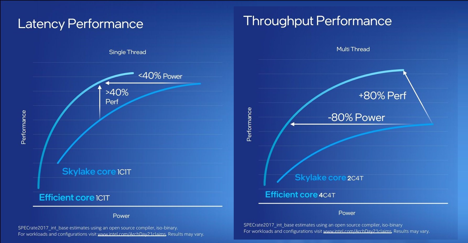
By these graphics it looks like that for peak single thread, we should see around +8% better than Skylake performance while consuming just over half the power – look for Cinebench R20 scores for one Gracemont thread around 478 then (Skylake 6700K scored 443). With +8% for single thread in mind, the +80% in MT comparing 4 cores of Gracemont to two fully loaded Skylake cores seems a little low – we’ve got double the physical cores with Gracemont compared to Skylake here. But there’s likely some additional performance regression with the cache structure on the new Atom core, which we’ll get to later on this page.
These claims are substantial. Intel hasn’t compared the new Atom core generation on generation, because it felt that having AVX2 support would put the new Atom at a significant advantage. But what Intel is saying with these graphs is that we should expect better-than Skylake performance at much less power. We saw Skylake processors up to 28 cores in HEDT – it makes me wonder if Intel might not enable its new Atom core for that market. If that’s the case, where is our 64-core Atom version for HEDT? I’ll take one.
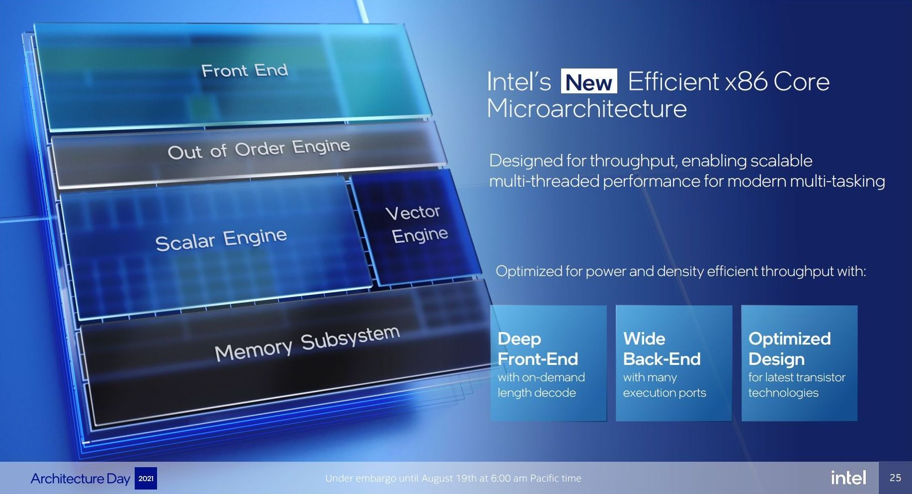
Front End
The big item about the Tremont front end of the core was the move to dual three-wide decode paths, enabling two concurrent streams of decode that could support 3 per cycle. That still remains in Gracemont, but is backed by a double-size 64 KB L1 Instruction cache. This ties into the branch predictor which enables prefetchers at all cache levels, along with a 5000-entry branch target cache which Intel says in improved over the previous generation.
Back on the decoder, Intel supports on-demand decode which stores a history of previous decodes in the instruction cache and if recent misses are recalled at the decode stage, the on-demand stream will pull directly from the instruction cache instead, saving time – if the prefetch/decode works, the content in the instruction cache is updated, however if it is doing poorly then the scope is ‘re-enabled for general fetches’ to get a better understanding of the instruction flow. This almost sounds like a micro-op cache without having a physical cache, but is more to do about instruction streaming. Either way, the decoders can push up to six uops into the second half of the front end.
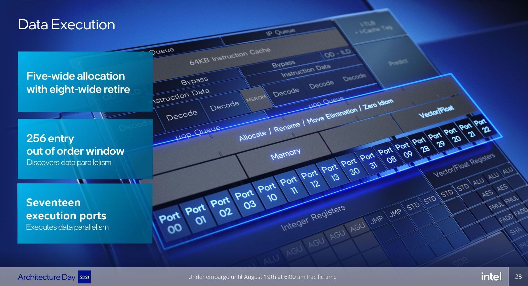
For Gracemont, the reorder buffer size has increased from 208 in Tremont to 256, which is important aspect given that Gracemont now has a total of 17 (!) execution ports, compared to eight in Tremont. This is also significantly wider than the execution capabilities of Golden Cove's 12 ports, related to the disaggregated integer and FP/vector pipeline design. However, despite that width, the allocation stage feeding into the reservation stations can only process five instructions per cycle. On the return path, each core can retire eight instructions per cycle.
Back End
So it’s a bit insane to have 17 execution ports here. There are a lot of repeated units as well, which means that Gracemont is expecting to see repeated instruction use and requires the parallelism to do more per cycle and then perhaps sit idle waiting for the next instructions to come down the pipe. Overall we have
- 4 Integer ALUs (ALU/Shift), two of which can do MUL/DIV
- 4 Address Generator Units, 2 Load + 2 Store
- 2 Branch Ports
- 2 Extra Integer Store ports
- 2 Floating Point/Vector store ports
- 3 Floating Point/Vector ALUs: 3x ALUs, 2x AES/FMUL/FADD, 1x SHA/IMUL/FDIV
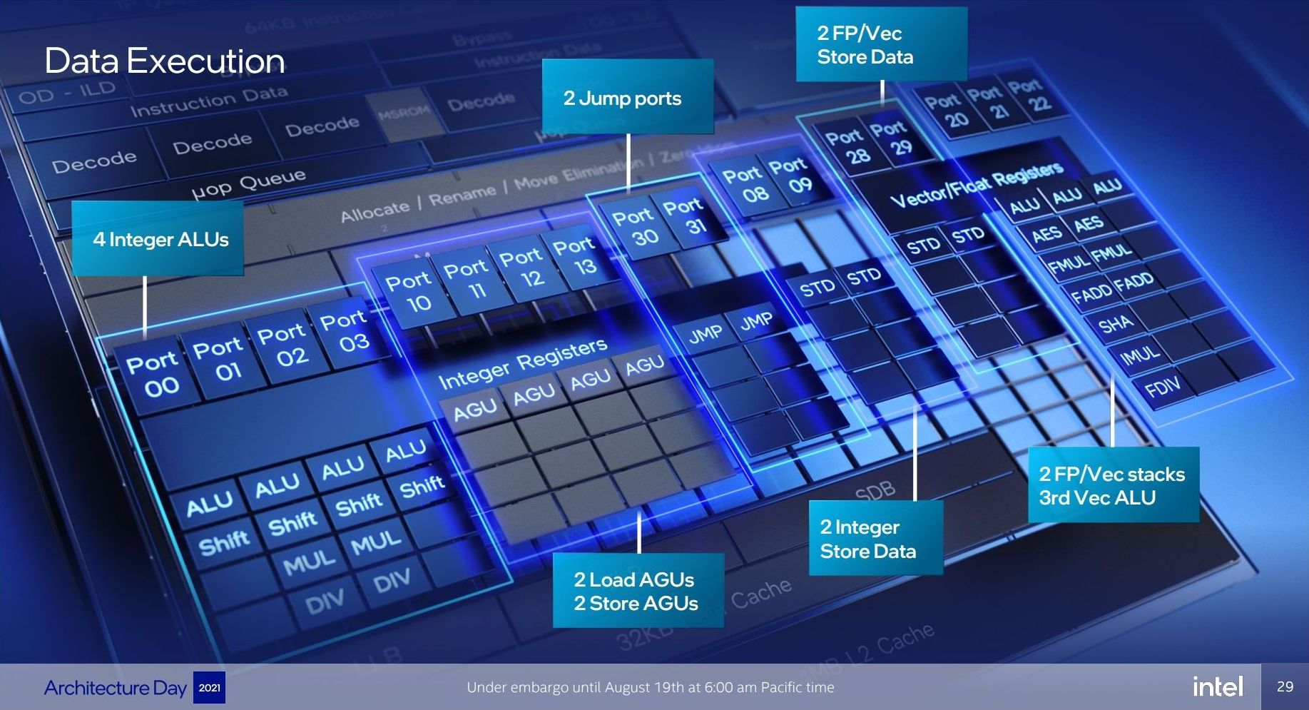
It will be interesting to see exactly how many of these can be accessed simultaneously. In previous core designs a lot of this functionality would be enabled though the same port – even Alder Lake’s P-core only has 12 execution ports, with some ports doing double duty on Vector and Integer workloads. In the P-core there is a single scheduler for both types of workloads, whereas in the E-core there are two separate schedulers, which is more akin to what we see on non-x86 core designs. It’s a tradeoff in complexity and ease-of-use.
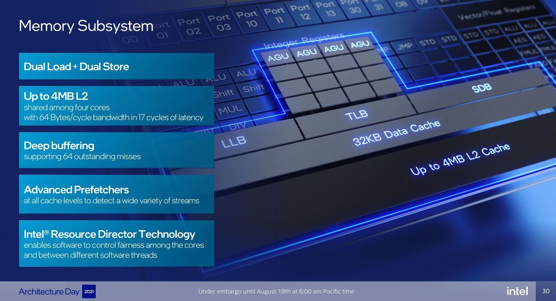
The back-end is support by a 32 KiB L1-Data cache, which supports a 3-cycle pointer chasing latency and 64 outstanding cache misses. There are two load and two store ports, which means 2x16 byte loads and 2 x 16 byte stores to the L1-D.
There is also has a shared 4 MB L2 cache across all four E-cores in a cluster with 17-cycle latency. The shared L2 cache can support 64 bytes per cycle read/write per core, which Intel states is sufficient for all four cores. The new L2 supports up to 64 outstanding misses to the deeper memory subsystem – which seems fair, but has to be shared amongst the 4 cores.
Intel states that it has a Resource Director that will arbitrate cache accesses between the four cores in a cluster to ensure fairness, confirming that Intel are building these E-cores in for multi-threaded performance rather than latency sensitive scenarios where one thread might have priority.
Other Highlights
As the first Atom core to have AVX2 enabled, there are two vector ports that support FMUL and FADD (port 20 and port 21), which means that we should expect peak performance compared to previous Atoms to be substantial. The addition of VNNI-INT8 over the AVX unit means that Intel wants these E-cores to enable situations where high inference throughput is needed, such as perhaps video analysis.
Intel was keen to point out that Gracemont has all of its latest security features including Control Flow Enhancement Technology (CET), and virtualization redirects under its VT-rp feature.
Overall, Intel stated that the E-cores are tuned for voltage more than anything else (such as performance, area). This means that the E-cores are set to use a lot less power, which may help in mobile scenarios. But as mentioned before on the first page, it will depend on how much power the ring has to consume in that environment - it should be worth noting that each four core Atom cluster only has a single stop on the full ring in Alder Lake, which Intel says should not cause congestion but it is a possibility – if each core is fully loaded, there is only 512 KB of L2 cache per core before making the jump to main memory, which indicates that in a fully loaded scenario, that might be a bottleneck.


223 Comments
View All Comments
name99 - Thursday, August 19, 2021 - link
"Intel’s Thread Director controller puts an embedded microcontroller inside the processor such that it can monitor what each thread is doing and what it needs out of its performance metrics. It will look at the ratio of loads, stores, branches, average memory access times, patterns, and types of instructions."People might be interested to know that Apple has done this for years (I don't know about ARM).
The Apple scheme has many moving parts but these include
- tracking how much work is done by Fetch, Decode and Execute. The first two can estimate based on number of instructions, the third takes account of the type of instruction.
- the scheme is even sophisticated enough (at least the patent talks about this) that the weights given to each of these pieces are variable to match the characteristics of the manufactured chip. Each SoC is tested and the precise weights are fused into the chip after testing.
- this mean that the SoC can calculate things like instantaneous power usage. This is used at the overall SoC level (to limit battery current draw) and at the per execution unit level (eg to halt the SIMD pipeline for a cycle every few cycles if some thermal pr power constraint is being exceeded). You will notice this is the equivalent of Intel's frequency throttling for AVX512, but much nicer because it is done on demand, purely to the level needed, and without slowing down the rest of the core or without a slow transition between faster and slower frequencies.
- there is also tracking of where L1 cache fills comes from. If a lot come from the E cores, the E-core frequency is boosted. If a lot come from DRAM, then the fabric frequency and DRAM frequency are boosted.
- behind everything, for *most purposes* the primary metric is nJ/instruction. The scheduler does many things in the obvious way you would expect (background threads on E cores, track progress vs deadline and ramp core performance up or down depending on how that is doing); but some non-obvious things are that code that is inefficient (ie nJ/instruction is too low) and that is not otherwise protected by the OS will be pushed to lower frequency or to an E-core. This might sound bad, but mainly what it's saying is
+ if you're constantly waiting on DRAM, then running the core at high frequency does you no good anyway
+ if you're not running very wide (hard to predict branches, or long dependency chains) you can't take advantage of the big core anyway, so why waste power keeping you there?
Presumably Intel's scheme at least covers all these sorts of bases.
One complication Apple has, that I assume Intel/Windows will not have (but it's not clear) is the use of clustering. Clustering sounds great, as does that huge low latency shared cache. But it comes at the cost of, as far as I can tell, a common frequency for the entire cluster. (If CPUs were at different frequencies, there'd have to be a cross-frequency-domain stage when communicating with the shared L2, at that would add noticeable latency).
So the OS scheduler doesn't just have the job of scheduling each thread to the optimal core at optimal DVFS, it also has to pack 4 optimal [as a unit] threads to a cluster...
I can't tell if Intel's scheme runs their small cores that way, as a cluster of 4 sharing an L2 (and thus sharing frequency). If so, how the OS scheduler handles this is something to keep an eye on for both Windows and Linux.
BTW there are very recently published patents that suggest Apple may be moving away from this, to a scheme of private L2s and a shared per-cluster L3!
https://patents.google.com/patent/US10942850B2
That's something to keep an eye on for the A15 and M2...
mode_13h - Friday, August 20, 2021 - link
Thanks for the info.What do you mean by "nJ/instruction" ? Is that the ratio of branches vs. non-branch instructions? If not, then what does it have to do with DRAM latency? Or was that a reference to the prior paragraph?
Where do you read this stuff?
name99 - Friday, August 20, 2021 - link
nanoJoules/instruction. ie energy per instructionThis info is acquired from reading massive numbers of Apple patents, validated as much as possible by experiments run on M1.
mode_13h - Saturday, August 21, 2021 - link
Wow. My eyes glaze over, trying to read patents. I'm sure there are better and worse ones, but they're often written in ways that drain the joy out of the most interesting ideas.Thanks for sharing!
jospoortvliet - Sunday, August 22, 2021 - link
Indeed super interesting!mode_13h - Thursday, August 19, 2021 - link
I wonder if they did anything to the decoder around SMT or multiple instruction streams. In Tremont, it seemed like they way they used a 6-wide decoder was as two 3-wide decoders, where each would work on a separate branch target.> the L2 BTB (branch target buffer) has grown to well over double with the
> structure increased from 5K entries to 12K entries
Can someone refresh us on the function of a BTB? Is it like a cache that stores the target address of each recent branch instruction, so that speculative execution doesn't have to wait for the target to be computed (if not a fixed target)?
> actually eliminating instructions that otherwise would have to actually
> emitted to the back-end execution resources.
Huh? Seems like an editing error. Can anyone elaborate?
> Intel still continues to use merged execution port / reservation station design
Someone please remind us what a reservation station is?
> On the integer side of things, there’s now a fifth execution port and pipeline with
> simple ALU and LEA capabilities
In this case, I presume LEA means "load effective address" and is used to compute memory addresses (potentially involving a multiply, an add, a constant offset?). Is that correct? And does the above statement mean that each of those ports can do simple ALU *or* LEA operations?
> Intel has improved the prefetchers
Yes, and the article text didn't even mention the bullet point in the slide about feedback-based prefetch-throttling! I'm reminded of how ARM's N2 can throttle back prefetching, during periods of memory contention. Perhaps Intel came to the same conclusion that overzealous prefetchers can starve cores running memory-intensive routines, in highly-threaded workloads.
> full-line-write predictive bandwidth optimisation ... where the core can greatly improve
> bandwidth by avoiding RFO reads of cache lines that are going to be fully rewritten
Yes, I've been wanting this for about 2 decades.
> We can see in the graph ... low outliers where the new design doesn’t improve thing
> much or even sees regressions, which is odd.
Maybe those were affected by the disabling of AVX-512? Or were those benchmarks performed on a fully-enabled core?
> +25% wider µOP output
If this is referring to expanding uOP cache outputs from 6 -> 8, that's a 33% improvement!
name99 - Thursday, August 19, 2021 - link
"Can someone refresh us on the function of a BTB? "It's hard to be sure because I can never tell the extent to which Intel is doing things the old comfortable way, or the most sensible new way. I'll tell you what Apple do.
Intel are presumably a subset of these features, but I don't know how good a subset. You need ALL the pieces to run sustained "random" code 8-wide as Apple does.
(a) You want a predictor for indirect branches (think things like virtual function or procPtr calls). How to construct such a predictor is interesting but we will just assume it exists. This may have been what the original Branch Target Buffer was say in the early 1990s, but it is NOT what we have in mind today.
(b) To run a modern wide OoO machine optimally, you want to be able to process a TAKEN branch per cycle. (Code has a branch every ~6 instructions, a taken branch every ~10 instructions. If you want to run 8 wide...)
- This means you need to pull a new run of instructions (ie loaded from a new address) every cycle.
- This, in turn, means that you really need to run Fetch as an asynchronous process. A Fetch Engine every cycle predicts the next Fetch Address and the number of instructions to Fetch. (On Apple this can be at least as wide as 16 instructions in one cycle if everything lines up correctly.) These instructions are placed in the Fetch Queue and at the other end Decode reads 8/cycle from this queue. Making Fetch async from the rest of the machine means that you can sometimes pull in 16 instructions into the queue, sometimes you just pull in three or four instructions, sometimes none while you wait for a cache miss. But hopefully the queue between Fetch and Decode buffers much of this variation.
- BUT asynchronous Fetch means Fetch is on its own regarding how it proceeds. Basically what you want is
+ a very fast (single cycle!) Next Fetch Predictor that produces the next fetch address and (ideally) also a Fetch Width
But a fast such predictor is of limited accuracy.
So the second essential you need is very high quality predictors that correct the Next Fetch Predictor. As long as you correct a misFetch before the instruction stream hits Rename life is fairly easy. Correcting after Rename is tough (you have to undo resource allocations), correcting after Issue is hopeless and you have to flush.
The Apple numbers are that their high quality predictors (Branch Prediction and Indirect Branch Prediction) are TAGE based, phenomenally accurate, and take up to 5 cycles to generate a result. That just works out (of course!)
So the idea is that the Next Fetch Predictor generates a stream of Fetch's which results in a stream of, let's call them cars of instructions, proceeding from I-cache, through the Fetch Queue, through Decode. At any point one of the better quality predictors can step in and derail all the cars after a certain point, so that Fetch restarts. Obviously this isn't great, you've lost up to five cycles of work, but it's a lot better than a full machine flush!
OK, within this framework, I believe that what Intel today calls the BTB is essentially doing the same job as what I am calling the Next Fetch Predictor.
BTW there are an insane number of tweaks and improvement Apple have made to the above scheme over the years. These include
- a separate Return stack used by the Next Fetch predictor to deal with extremely rapid call/return pairs (eg call, work, return is three cycles; all done before the code has even hit decode, so totally out of sync with the "full accuracy" Return stack)
- Decode (ie the earliest stage possible) does what it can to keep the machinery on track. Decode detects any sort of mismatch between decoded branches and the next car of instructions and, if so, gets Fetch to resteer. This is easily done for unconditional branches, and can also be done for a few other weird cases (like some mismatched call/return pairs). Decode also updates the Return stack.
- pre-decode (ie when an instruction line is moved from l2 to L1) does a bunch of stuff to mark significant points (eg where branches are) in a cache line. This in turn is referenced the first time the Next Fetch Predictor encounters these new lines.
- for certain cases (most obviously when the Next Fetch Predictor has an indirect branch marked as low confidence) Fetch pauses until some of the upstream machinery can suggest an address. The idea is that for low confidence indirect branches, you're so unlikely to guess correctly why even waste energy trying?
Apart from all these, theres a whole other set of machinery that handles loops and the transition from "random" code to loops. These include both an L0 cache and a trace cache. (That's right kids, a trace cache!)
There's also a whole set of ideas for saving power at every stage of this process. For example the Next Fetch Predictor, along with the obvious things it is recording (next fetch address, and fetch width) also records two items obvious in retrospect -- the physical address (so no TLB lookup necessary) and even the cache way (so no way prediction necessary, and the correct way -- and only that way) can be fired up on cache access. The loop buffer, L0, and the trace cache are additional ways to run Fetch on energy fumes for code that meets the specific requirements, so that various of TLB, way prediction, multi-way lookup, branch predictor, etc etc can all be powered down.
mode_13h - Friday, August 20, 2021 - link
Thanks for the info. I wonder where you find such detailed descriptions!> L0 cache
Just another name for a uop cache?
> That's right kids, a trace cache!
So, a trace cache stores an entire string of instructions, even across one or more branches? Does it hold instructions before or after decode?
> and even the cache way
You mean the cache set?
> The loop buffer
What's a loop buffer? Sort of like a trace cache, for loops?
name99 - Friday, August 20, 2021 - link
Think of the steps required to run normal code, as I described above. The consider various simple loops.Suppose you have a straight line loop, say 40 instructions in the loop body, no branches. Then you can omit branch prediction, TLB, cache -- just repeatedly run the same code from a straight buffer. That's essentially a loop buffer.
Now suppose that your loop body has a few branches in it, but they are predictable, maybe something like
if(loop counter even){path1} else {path2}
Now what you want is something like a trace cache that's holding the two paths path1 and path2, and a very simple predictor that's telling which of these to choose each iteration. You can still avoid the costs of a real branch predictor and a real cache.
Now suppose you have a loop with moderately complicated branches, not terrible but not that easy to predict either. You can't avoid the cost of branch prediction now (as I said, to validate the guess of the Next Fetch Predictor) but you can avoid much of the cost of the cache by moving the loop body into an L0 cache which will be essentially a small direct-mapped cache. Being smaller, and direct-mapped, it will use less energy/access than the full I-cache. (And you probably will also access it virtually rather than physically, so also avoid TLB costs.)
cache way:
Recall that a DIRECT-MAPPED cache has only a single place where a line can go -- grab some bits from the middle of an address, they define an index, the line goes at that index. This is fast and cheap, but means you have a problem if you frequently want to access two addresses with the same index (ie same middle bits in their addresses).
n-way set-associative cache means you now have, n (may be 2, 4, 8 or some other number) of slots associated with a given index. So if you have 8 slots, you can hold 8 lines with that same index, ie 8 addresses with those same middle bits.
BUT how do you know WHICH of those 8 lines you want? Ahh.
That gets into the business of matching tags, way prediction and a whole mess of other stuff that you need to read in a textbook. But the relevance to what I was saying is that which of these 8 possible lines is of interest is called a WAY. So by storing the cache way, you can access a cache with the speed (avoid cache tag lookup) and energy (no need to precharge the tags) of a direct-mapped cache.
GeoffreyA - Saturday, August 21, 2021 - link
Great information. I believe on the Intel side, Nehalem added something like that, the LSD.