Intel Architecture Day 2021: Alder Lake, Golden Cove, and Gracemont Detailed
by Dr. Ian Cutress & Andrei Frumusanu on August 19, 2021 9:00 AM ESTGracemont Microarchitecture (E-Core) Examined
The smaller core as part of Intel’s hybrid Alder Lake design is called an E-core, and is built on the Gracemont microarchitecture. It forms part of Intel’s Atom family of processors, and is a significant microarchitectural jump over the previous Atom core design called Tremont.
- 2008: Bonnell
- 2011: Saltwell
- 2013: Silvermont
- 2015: Airmont
- 2016: Goldmont
- 2017: Goldmont Plus
- 2020: Tremont
- 2021: Gracemont
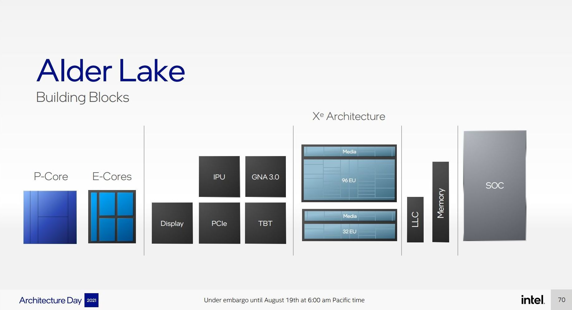
Based on Intel’s diagrams, the company is pitching that the size of its Golden Cove core means that in the space it would normally fit one of its P-core designs, it can enable a four core cluster of E-cores along with a shared 4MB L2 cache between them.
For performance, Intel has some pretty wild claims. It splits them up into single thread and multi-thread comparisons using SPECrate2017_int.
When comparing 1C1T of Gracemont against 1C1T of Skylake, Intel’s numbers suggest:
- +40% performance at iso-power (using a middling frequency)
- 40% less power* at iso-performance (peak Skylake performance)
*'<40%' is now stood to mean 'below 40 power'
When comparing 4C4T of Gracemont against 2C4T of Skylake, Intel’s numbers suggest:
- +80% performance peak vs peak
- 80% less power at iso performance)peak Skylake performance
We pushed the two Intel slides together to show how they presented this data.
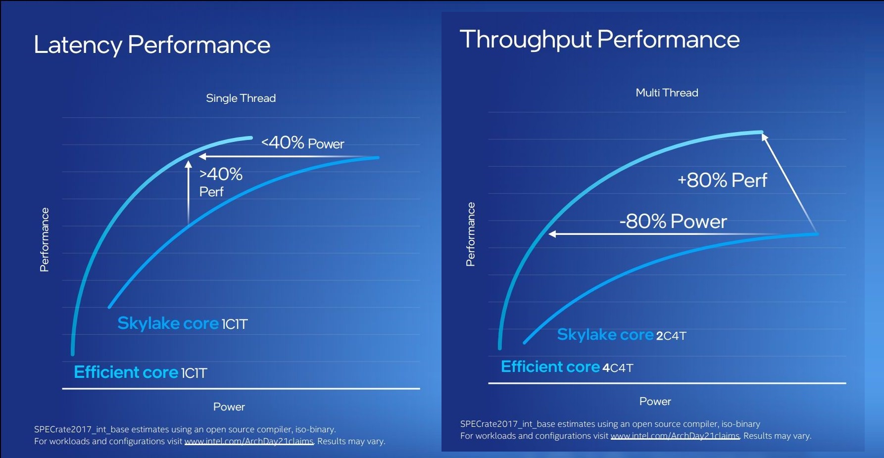
By these graphics it looks like that for peak single thread, we should see around +8% better than Skylake performance while consuming just over half the power – look for Cinebench R20 scores for one Gracemont thread around 478 then (Skylake 6700K scored 443). With +8% for single thread in mind, the +80% in MT comparing 4 cores of Gracemont to two fully loaded Skylake cores seems a little low – we’ve got double the physical cores with Gracemont compared to Skylake here. But there’s likely some additional performance regression with the cache structure on the new Atom core, which we’ll get to later on this page.
These claims are substantial. Intel hasn’t compared the new Atom core generation on generation, because it felt that having AVX2 support would put the new Atom at a significant advantage. But what Intel is saying with these graphs is that we should expect better-than Skylake performance at much less power. We saw Skylake processors up to 28 cores in HEDT – it makes me wonder if Intel might not enable its new Atom core for that market. If that’s the case, where is our 64-core Atom version for HEDT? I’ll take one.
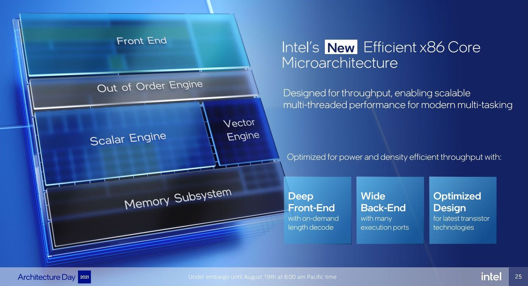
Front End
The big item about the Tremont front end of the core was the move to dual three-wide decode paths, enabling two concurrent streams of decode that could support 3 per cycle. That still remains in Gracemont, but is backed by a double-size 64 KB L1 Instruction cache. This ties into the branch predictor which enables prefetchers at all cache levels, along with a 5000-entry branch target cache which Intel says in improved over the previous generation.
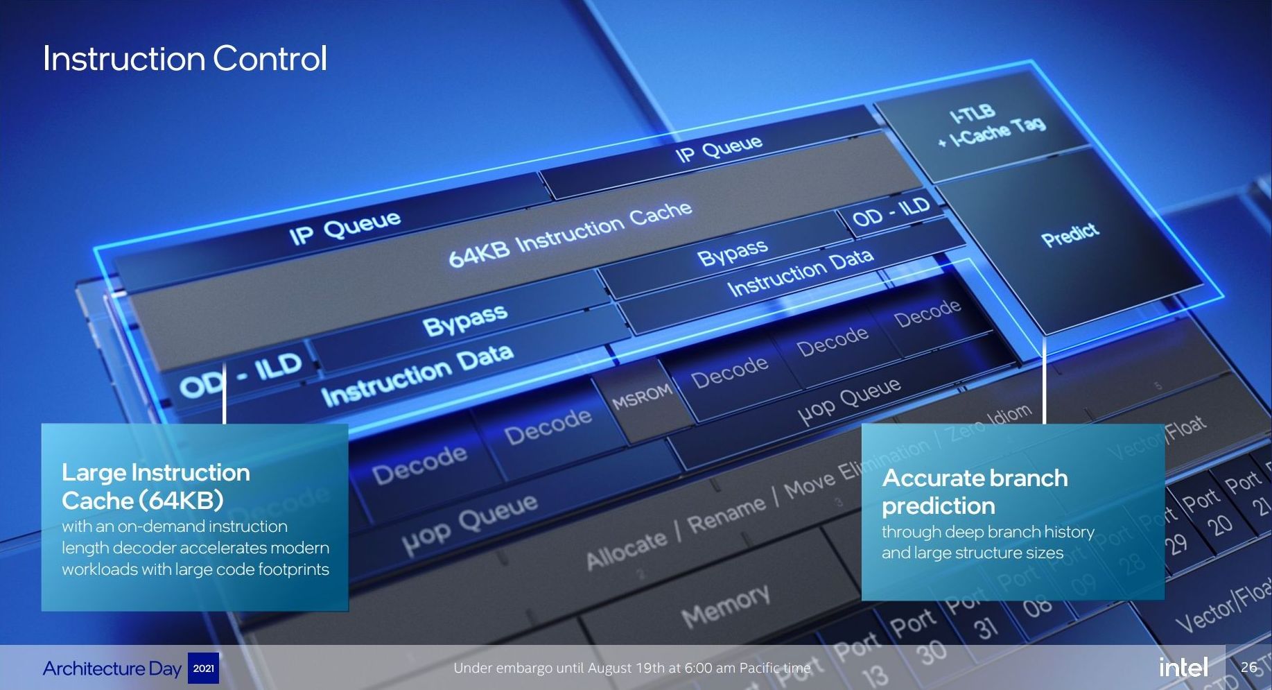
Back on the decoder, Intel supports on-demand decode which stores a history of previous decodes in the instruction cache and if recent misses are recalled at the decode stage, the on-demand stream will pull directly from the instruction cache instead, saving time – if the prefetch/decode works, the content in the instruction cache is updated, however if it is doing poorly then the scope is ‘re-enabled for general fetches’ to get a better understanding of the instruction flow. This almost sounds like a micro-op cache without having a physical cache, but is more to do about instruction streaming. Either way, the decoders can push up to six uops into the second half of the front end.
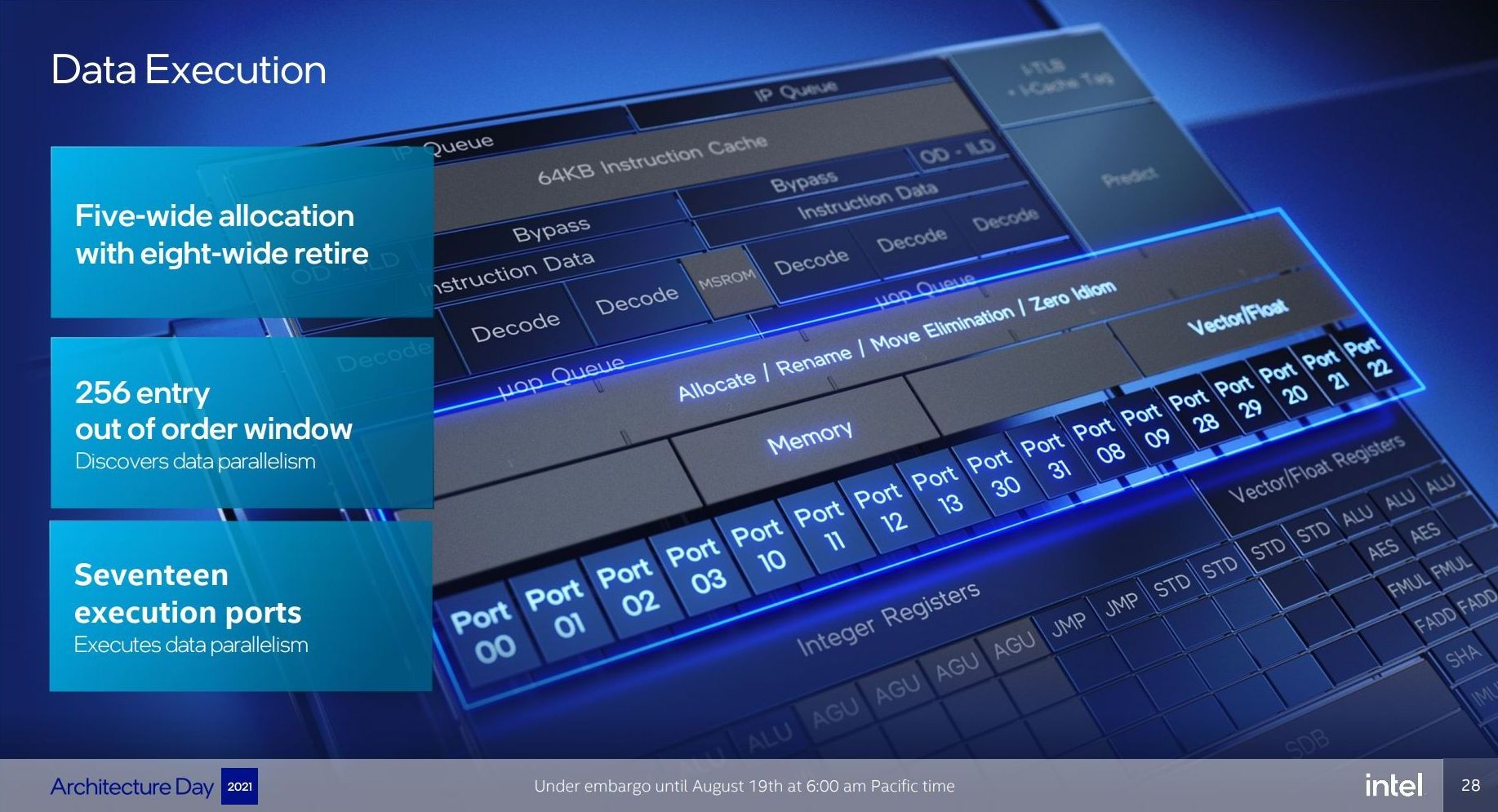
For Gracemont, the reorder buffer size has increased from 208 in Tremont to 256, which is important aspect given that Gracemont now has a total of 17 (!) execution ports, compared to eight in Tremont. This is also significantly wider than the execution capabilities of Golden Cove's 12 ports, related to the disaggregated integer and FP/vector pipeline design. However, despite that width, the allocation stage feeding into the reservation stations can only process five instructions per cycle. On the return path, each core can retire eight instructions per cycle.
Back End
So it’s a bit insane to have 17 execution ports here. There are a lot of repeated units as well, which means that Gracemont is expecting to see repeated instruction use and requires the parallelism to do more per cycle and then perhaps sit idle waiting for the next instructions to come down the pipe. Overall we have
- 4 Integer ALUs (ALU/Shift), two of which can do MUL/DIV
- 4 Address Generator Units, 2 Load + 2 Store
- 2 Branch Ports
- 2 Extra Integer Store ports
- 2 Floating Point/Vector store ports
- 3 Floating Point/Vector ALUs: 3x ALUs, 2x AES/FMUL/FADD, 1x SHA/IMUL/FDIV
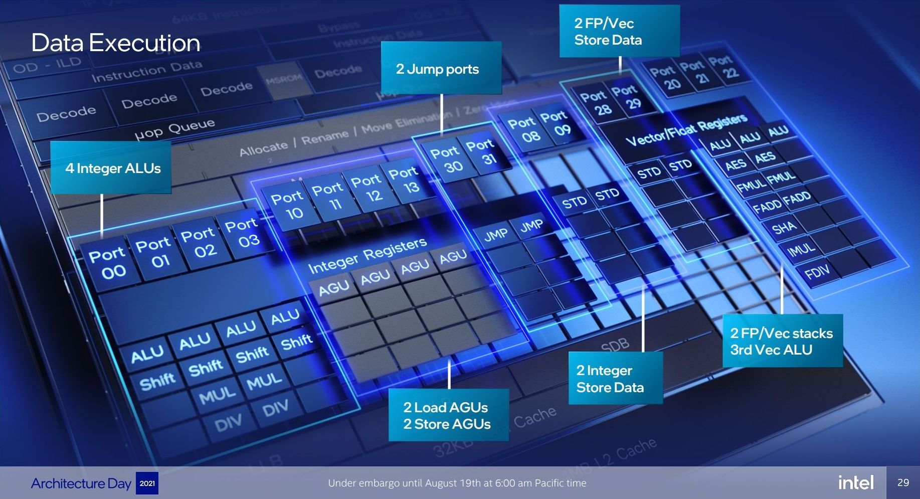
It will be interesting to see exactly how many of these can be accessed simultaneously. In previous core designs a lot of this functionality would be enabled though the same port – even Alder Lake’s P-core only has 12 execution ports, with some ports doing double duty on Vector and Integer workloads. In the P-core there is a single scheduler for both types of workloads, whereas in the E-core there are two separate schedulers, which is more akin to what we see on non-x86 core designs. It’s a tradeoff in complexity and ease-of-use.
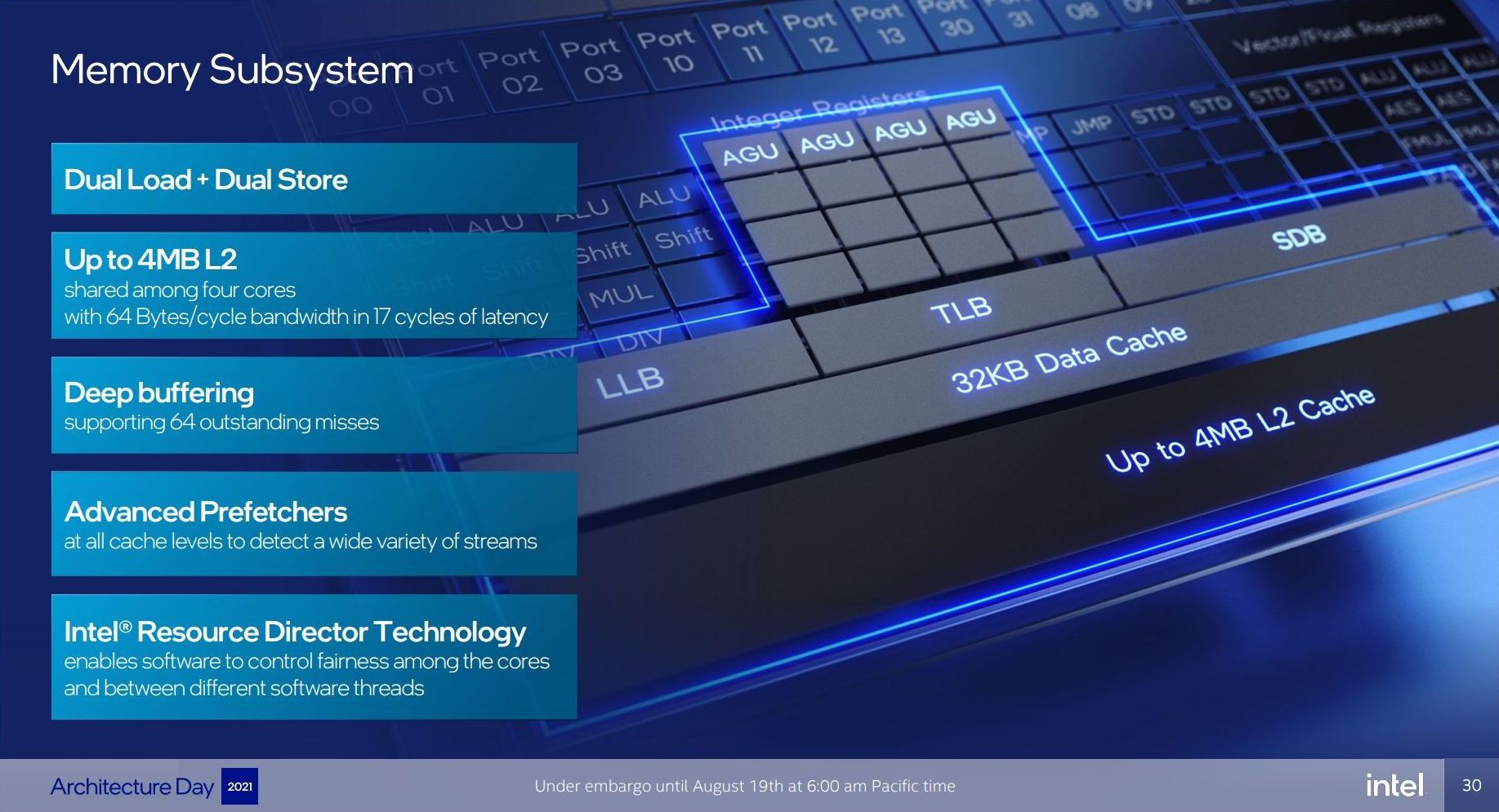
The back-end is support by a 32 KiB L1-Data cache, which supports a 3-cycle pointer chasing latency and 64 outstanding cache misses. There are two load and two store ports, which means 2x16 byte loads and 2 x 16 byte stores to the L1-D.
There is also has a shared 4 MB L2 cache across all four E-cores in a cluster with 17-cycle latency. The shared L2 cache can support 64 bytes per cycle read/write per core, which Intel states is sufficient for all four cores. The new L2 supports up to 64 outstanding misses to the deeper memory subsystem – which seems fair, but has to be shared amongst the 4 cores.
Intel states that it has a Resource Director that will arbitrate cache accesses between the four cores in a cluster to ensure fairness, confirming that Intel are building these E-cores in for multi-threaded performance rather than latency sensitive scenarios where one thread might have priority.
Other Highlights
As the first Atom core to have AVX2 enabled, there are two vector ports that support FMUL and FADD (port 20 and port 21), which means that we should expect peak performance compared to previous Atoms to be substantial. The addition of VNNI-INT8 over the AVX unit means that Intel wants these E-cores to enable situations where high inference throughput is needed, such as perhaps video analysis.
Intel was keen to point out that Gracemont has all of its latest security features including Control Flow Enhancement Technology (CET), and virtualization redirects under its VT-rp feature.
Overall, Intel stated that the E-cores are tuned for voltage more than anything else (such as performance, area). This means that the E-cores are set to use a lot less power, which may help in mobile scenarios. But as mentioned before on the first page, it will depend on how much power the ring has to consume in that environment - it should be worth noting that each four core Atom cluster only has a single stop on the full ring in Alder Lake, which Intel says should not cause congestion but it is a possibility – if each core is fully loaded, there is only 512 KB of L2 cache per core before making the jump to main memory, which indicates that in a fully loaded scenario, that might be a bottleneck.


223 Comments
View All Comments
mode_13h - Friday, August 20, 2021 - link
Yeah, we get it. That's their standard chromebook-level SoC, actually. Check out Jasper Lake:https://ark.intel.com/content/www/us/en/ark/produc...
mode_13h - Friday, August 20, 2021 - link
> Why not an SoC with 4, 6, or 8 Gracemont cores plus some Xe GraphicsIf history is any guide, Intel will *certainly* release low-end CPUs with only Gracemont cores. I'm not sure if they'll do the 6-core or 8-core variants, but definitely 4-core + probably a 32-EU Xe iGPU.
ifThenError - Friday, August 20, 2021 - link
+1 for a high-core-count-small-core chip!It's a shame the current Snow Ridge chips are not available to consumers. That leaves only Ryzen U-series for multithreaded energy aware computing. Not saying these are bad, but an alternative wouldn't hurt.
mode_13h - Saturday, August 21, 2021 - link
> +1 for a high-core-count-small-core chip!They already do that. The Atom-branded processors currently ship in up to 24-core configurations, targeted at applications like 5G basestations. The Snow Ridge you mention are based on Tremont cores:
https://ark.intel.com/content/www/us/en/ark/produc...
Interestingly, it's limited to just dual-channel DDR4, but it has 32-lanes of PCIe 3.0 support. Presumably, a refresh with Gracemont would use DDR5 and at least PCIe 4.0.
> It's a shame the current Snow Ridge chips are not available to consumers.
Well, they're BGA. So, you probably don't want a bare CPU. What you'd need to find is someone selling them on boards in a standard PC form factor. I already checked Supermicro, but their Atom boards feature older models. Didn't find anything from ASRock Rack or Gigabyte, either.
ifThenError - Saturday, August 21, 2021 - link
And that is exactly the point. I know there are CPUs with more Atom cores out there, and I'd be perfectly fine with a small mainboard with soldered chip or a NUC type barebone. But they are simply not sold to consumers and this is one major disappointment.The consumer line just ends with the 4 cores and everything else is big cores, bigger coolers junk.
mode_13h - Sunday, August 22, 2021 - link
Well, you can find boards with higher core-count Atoms, but I just didn't see any with Snow Ridge. Maybe it's just a matter of time, or maybe we'd need to look a little harder.ifThenError - Sunday, August 22, 2021 - link
Do you have an example? The only ones I'm aware of are with totally outdated cores like Apollo Lake...mode_13h - Monday, August 23, 2021 - link
Well, here are some boards with Atom C-series, but I think they're still featuring Goldmont/Goldmont+ cores.https://www.supermicro.com/products/motherboard/At...
The biggest they have is based on the 16-core C3958. I'd keep an eye out, to see if they release a new generation with the newer Tremont-based P-series.
ifThenError - Monday, August 23, 2021 - link
Yes these are the ones I meant. Mixed up the names though, they are not Apollo Lake, but Denverton, but still it's all Goldmont cores (not even Goldmont Plus). So they are already 2 generations behind and on a much inferior process node.Unfortunately I don't have hopes for a Tremont alternative. The current P-series are all without iGPU, so it's only for headless servers. I guess there's little chance we'll see any systems available with these chips any time soon...
mode_13h - Tuesday, August 24, 2021 - link
> The current P-series are all without iGPUSo are the C-series!
If you want more than 4 cores, you're talking about a server SoC. So, that means getting it on a server board that will have a BMC anyhow.
If you're cool with a consumer version, then we can hope they up the core count of their Chromebook SoCs to 6 or 8, for Gracemont.