Intel Architecture Day 2021: Alder Lake, Golden Cove, and Gracemont Detailed
by Dr. Ian Cutress & Andrei Frumusanu on August 19, 2021 9:00 AM ESTConclusions
Alder Lake is set to come to market for both desktop and mobile, and we’re expecting the desktop hardware to start to appear by the end of the year – perhaps a little later for the rest of the family, but all-in-all we expect Intel is experiencing some serious squeaky bum time regarding how all the pieces will fit in place at that launch. The two main critical factors are operating systems and memory.
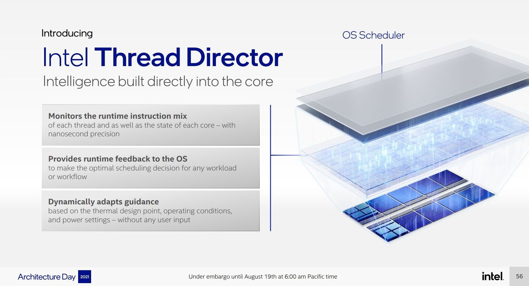
Because Alder Lake is Intel’s first full-stack attempt to commercialize a hybrid design, it has had to work closely with Microsoft to enable all the features it needs to make managing a hybrid core design properly beneficial to users. Intel’s new Thread Director Technology couples an integrated microcontroller per P-core and a new API for Windows 11 such that the scheduler in the operating system can take hints about the workflow on the core at a super fine granularity – every 30 microseconds or so. With information about what each thread is doing (from heavy AVX2 down to spin lock idling), the OS can react when a new thread needs performance, and choose which threads need to be relegated down to the E-core or as a hyperthread (which is classified as slower than an E-core).
When I first learned Alder Lake was going to be a hybrid design, I was perhaps one of the most skeptical users about how it was going to work, especially with some of the limits of Windows 10. At this point today however, with the explanations I have from Intel, I’m more confident than not that they’ve done it right. Some side off-the-record conversations I have had have only bolstered the idea that Microsoft has done everything Intel has asked, and users will need Windows 11 to get that benefit. Windows 10 still has some Hardware Guided Scheduling, but it’s akin to only knowing half the story. The only question is whether Windows 11 will be fully ready by the time Alder Lake comes to market.
For memory, as a core design, Alder Lake will have support for DDR4 and DDR5, however only one can be used at any given time. Systems will have to be designed for one or the other – Intel will state that by offering both, OEMs will have the opportunity to use the right memory at the right time for the right cost, however the push to full DDR5 would simplify the platform a lot more. We’re starting to see DDR5 come to the consumer market, but not in any volume that makes any consumer sense – market research firms expect the market to be 10% DDR5 by the end of 2022, which means that consumers might have to be stay with DDR4 for a while, and vendors will have to choose whether to bundle DDR5 with their systems. Either way, there’s no easy answer to the question ‘what memory should I use with Alder Lake’.
Through The Cores and The Atoms
From a design perspective, both the P-core and E-core are showcasing substantial improvements to their designs compared to previous generations.
The new Golden Cove core has upgraded the front-end decoder, which has been a sticking point for analysis of previous Cove and Lake cores. The exact details of how they operate are still being kept under wraps, but having a 6-wide variable length decoder is going to be an interesting talking point against 8-wide fixed-length decoders in the market and which one is better. The Golden Cove core also has very solid IPC figure gains, Intel saying 19%, although the fact there are some regressions is interesting. Intel did compare Golden Cove to Cypress Cove, the backported desktop core, rather than Willow Cove, the Tiger Lake core, which would have been a more apt comparison given that our testing shows Willow Cove slightly ahead. But still, around 19% is a good figure. Andrei highlights in his analysis that the move from a 10-wide to a 12-wide disaggregated execution back-end should be a good part of that performance, and that most core designs that go down this route end up being good.
However, for Gracemont, Intel has taken that concept to the extreme. Having 17 execution ports allows Intel to clock-gate each port when not in use, and even when you couple that with a smaller 5-wide allocation dispatch and 8-wide retire, it means that without specific code to keep all 17 ports fed, a good number are likely to be disabled, saving power. The performance numbers Intel provided were somewhat insane for Gracemont, suggesting +8% performance over Skylake at peak power, or a variety of 40% ST perf/power or 80% MT perf/power against Skylake. If Gracemont is truly a Skylake-beating architecture, then where have you been! I’m advocating for a 64-core HEDT chip tomorrow.
One harsh criticism Intel is going to get back is dropping AVX-512 for this generation. For the talk we had about ‘no transistor left behind’, Alder Lake dropped it hard. That’s nothing to say if the functionality will come back later, but if rumors are believed and Zen 4 has some AVX-512 support, we might be in a situation where the only latest consumer hardware on the market supporting AVX-512 is from AMD. That would be a turn-up. But AMD’s support is just a rumor, and really if Intel wants to push AVX-512 again, it will have a Sisyphean task to convince everyone it’s what the industry needs.
Where We Go From Here
There are still some unanswered questions as to the Alder Lake design, and stuff that we will test when we get the hardware in hand. Intel has an event planned for the end of October called the Intel InnovatiON event (part of the ON series), which would be the right time to introduce Alder Lake as a product to the world. Exactly when it comes to retail will be a different question, but as long as Intel executes this year on the technology, it should make for an interesting competition with the rest of the market.


223 Comments
View All Comments
mode_13h - Friday, August 20, 2021 - link
> - treat all-zero lines as special cases that are tagged in L2/SLC but don't require> transferring data on the NoC. Intel had something like this in IceLake that, after
> some time, they switched off with microcode update.
I heard about that. Sad to see it go, but certainly one of those micro-optimizations that's barely measurable.
name99 - Thursday, August 19, 2021 - link
" This is over double that of AMD’s Zen3 µarch, and really only second to Apple’s core microarchitecture which we’ve measured in at around 630 instructions. "Apple's ROB is in fact around 2300 entries in size. But because it is put together differently than the traditional ROB, you will get very different numbers depending on exactly what you test.
The essential points are
(a)
- the ROB proper consists of about 330 "rows" where each row holds 7 instructions.
- one of these instructions can be a "failable", ie something that can force a flush. In other words branches or load/stores
- so if you simply count NOPs, you'll get a count of ~2300 entries. Anything else will hit earlier limits.
(b) The most important of these limits, for most purposes, is the History File which tracks changes in the logical to physical register mapping. THIS entity has ~630 entries and is what you will bump into first if you test somewhat varied code.
Earlier limits are ~380 int physical registers, ~420 or so FP registers, ~128 flag registers. But if you balance code across fp and int you will hit the 630 History File limit first.
(c) If you carefully balance that against code that does not touch the History File (mainly stores and branches) than you can get to almost but not quite 1000 ROB entries.
The primary reason Apple looks so different from x86 is that (this is a common pattern throughout Apple's design)
- what has traditionally been one object (eg a ROB that tracks instruction retirement AND tracks register mappings) is split into two objects each handling a single task.
The ROB handles in-order retiring, including flush. The History File handles register mapping (in case of flush and revert to an earlier state) and marking registers as free after retire.
This design style is everywhere. Another, very different, example, is the traditional Load part of the Load/Store queue is split into two parts, one tracking overlap with pending/unresolved stores, the second part tracking whether Replay might be required (eg because of missing in TLB or in the L1).
- even a single object is split into multiple what Apple calls "slices", but essentially a way to share rare cases with common cases, so the ROB needs to track some extra state for "failable" instructions that may cause a flush, but not every instruction needs that state. So you get this structure where you have up to six "lightweight" instructions with small ROB slots, and a "heavyweight" instruction with a larger ROB slot. Again with see this sort of thing everywhere, eg in the structures that hold branches waiting to retire which are carefully laid out to cover lots of branches, but with less storage for various special cases (taken branches need to preserve the history/path vectors, none-taken branches don't; indirect branches need to store a target, etc etc)
GeoffreyA - Friday, August 20, 2021 - link
Thanks for all the brilliant comments on CPU design!mode_13h - Friday, August 20, 2021 - link
Go go go!GeoffreyA - Thursday, August 19, 2021 - link
I think Intel did a great job at last. Golden Cove, impressive. But the real star's going to be Gracemont. Atom's come of age at last. Better than Skylake, while using less power, means it's somewhere in the region of Zen 2. Got a feeling it'll become Intel's chief design in the future, the competitor to Zen.As for Intel Thread Director, interesting and impressive; but the closer tying of hardware and scheduler, not too sure about that. Name reminded me of the G-Man, strangely enough. AVX512, good riddance. And Intel Marketing, good job on the slides. They look quite nice. All in all, glad to see Intel's on the right track. Keep it up. And thanks for the coverage, Ian and Andrei.
Silver5urfer - Friday, August 20, 2021 - link
Lol. That is no star. The small puny SKL cores are not going to render your high FPS nor the Zip compression. They are admitting themselves these are efficiency. Why ? Because 10SF is busted in power consumption and Intel cannot really make any more big cores on their Desktop platform without getting power throttled. On top their Ring bus cannot scale like SKL anymore.GeoffreyA - Friday, August 20, 2021 - link
Not as it stands, but mark my words, the Atom design is going to end up the main branch, on the heels of Zen in p/w. Interesting ideas are getting poured into this thing, whereas the bigger cores, they're just making it wider for the most part.ifThenError - Friday, August 20, 2021 - link
Totally understand your point and I'd personally welcome such a development!Anyway, the past years have shown a rather opposite way. Just take ARM as an example. There once was an efficiency line of cores that got the last update years ago with the A35. Now it's labelled as "super efficient" and hardly has any implementations aside from devices sitting idle most of the time. You can practically consider it abandoned.
The former mid tier with the A55 is now marketed as efficient cores, while the former top tier A7x more and more turns into the new midrange. Meanwhile people go all crazy about the new X1 top tier processors even though the growth of power consumption and heat is disproportionate to the performance. Does this sound reasonable in a power and heat constraint environment? Yeah, I don't think so either! ;-)
For that reason I perfectly understand Ian's demand for a 64 core Gracemont CPU. Heck, even a 16 core would still be #1 on my wishlist.
GeoffreyA - Saturday, August 21, 2021 - link
Yes, performance/watt is the way to go, and I reckon a couple more rounds of iteration will get Atom running at the competition's level. The designs are similar enough. It's ironic, because Atom had a reputation for being so slow.mode_13h - Saturday, August 21, 2021 - link
> Atom had a reputation for being so slow.With Tremont, Intel really upped their Atom game. It added a lot of complexity and grew significantly wider.
However, it's not until Gracemont's addition of AVX/AVX2 that Intel is clearly indicating it wants these cores to be taken seriously.
I wonder if Intel will promote their Atom line of SoCs as the new replacement for Xeon D. Currently, I think they're just being marketed for embedded servers and 5G Basestations, but they seem to have the nous to taken the markets Xeon D was targeting.