Intel Architecture Day 2021: Alder Lake, Golden Cove, and Gracemont Detailed
by Dr. Ian Cutress & Andrei Frumusanu on August 19, 2021 9:00 AM ESTGracemont Microarchitecture (E-Core) Examined
The smaller core as part of Intel’s hybrid Alder Lake design is called an E-core, and is built on the Gracemont microarchitecture. It forms part of Intel’s Atom family of processors, and is a significant microarchitectural jump over the previous Atom core design called Tremont.
- 2008: Bonnell
- 2011: Saltwell
- 2013: Silvermont
- 2015: Airmont
- 2016: Goldmont
- 2017: Goldmont Plus
- 2020: Tremont
- 2021: Gracemont
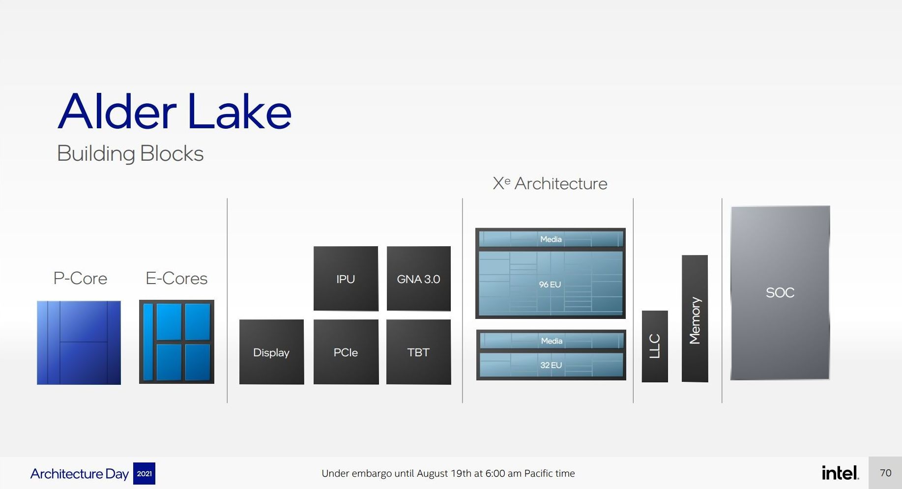
Based on Intel’s diagrams, the company is pitching that the size of its Golden Cove core means that in the space it would normally fit one of its P-core designs, it can enable a four core cluster of E-cores along with a shared 4MB L2 cache between them.
For performance, Intel has some pretty wild claims. It splits them up into single thread and multi-thread comparisons using SPECrate2017_int.
When comparing 1C1T of Gracemont against 1C1T of Skylake, Intel’s numbers suggest:
- +40% performance at iso-power (using a middling frequency)
- 40% less power* at iso-performance (peak Skylake performance)
*'<40%' is now stood to mean 'below 40 power'
When comparing 4C4T of Gracemont against 2C4T of Skylake, Intel’s numbers suggest:
- +80% performance peak vs peak
- 80% less power at iso performance)peak Skylake performance
We pushed the two Intel slides together to show how they presented this data.
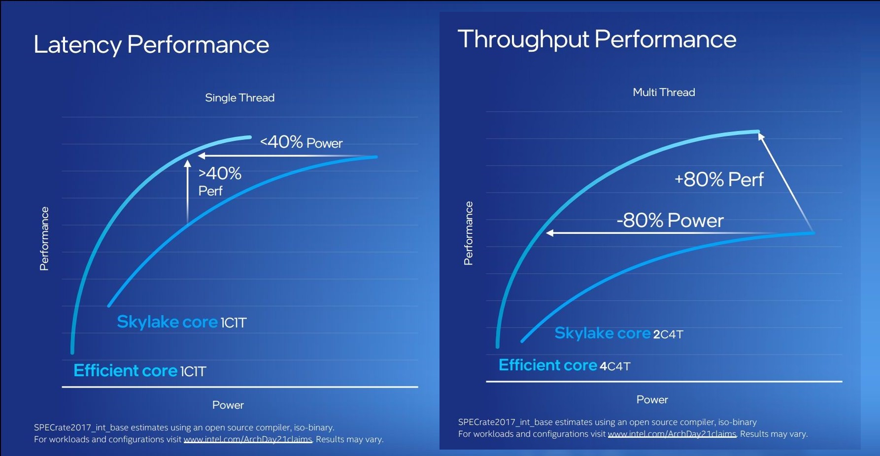
By these graphics it looks like that for peak single thread, we should see around +8% better than Skylake performance while consuming just over half the power – look for Cinebench R20 scores for one Gracemont thread around 478 then (Skylake 6700K scored 443). With +8% for single thread in mind, the +80% in MT comparing 4 cores of Gracemont to two fully loaded Skylake cores seems a little low – we’ve got double the physical cores with Gracemont compared to Skylake here. But there’s likely some additional performance regression with the cache structure on the new Atom core, which we’ll get to later on this page.
These claims are substantial. Intel hasn’t compared the new Atom core generation on generation, because it felt that having AVX2 support would put the new Atom at a significant advantage. But what Intel is saying with these graphs is that we should expect better-than Skylake performance at much less power. We saw Skylake processors up to 28 cores in HEDT – it makes me wonder if Intel might not enable its new Atom core for that market. If that’s the case, where is our 64-core Atom version for HEDT? I’ll take one.
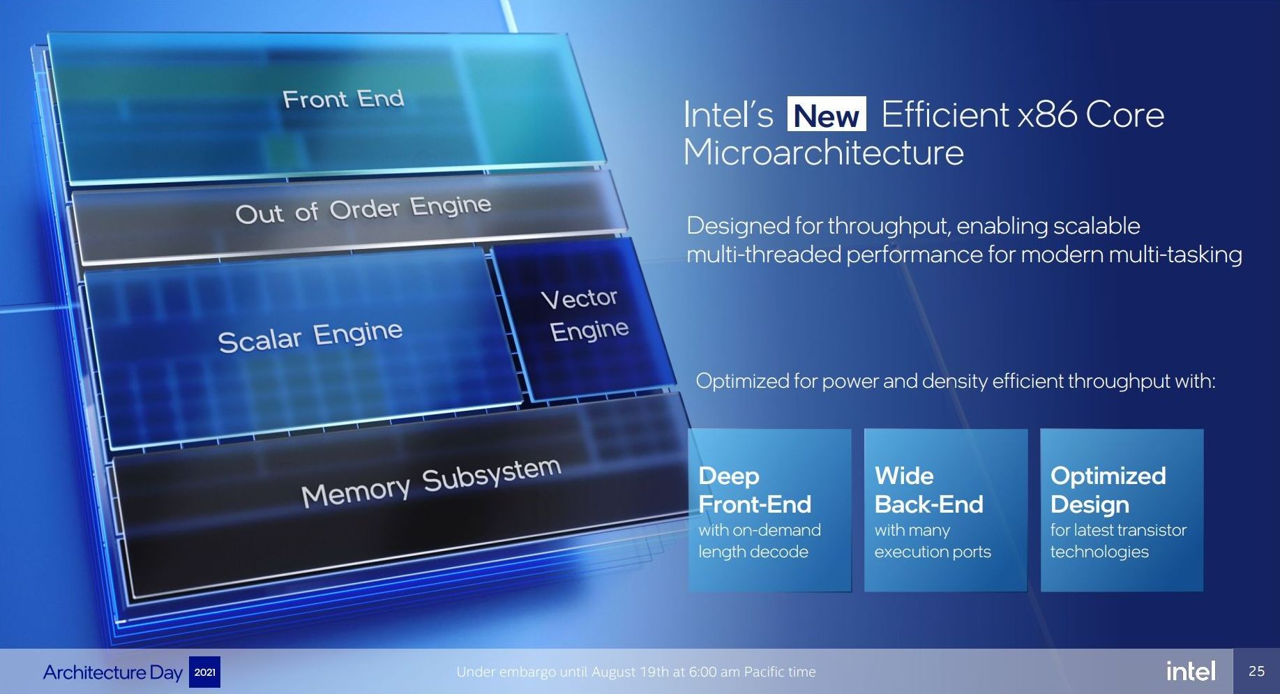
Front End
The big item about the Tremont front end of the core was the move to dual three-wide decode paths, enabling two concurrent streams of decode that could support 3 per cycle. That still remains in Gracemont, but is backed by a double-size 64 KB L1 Instruction cache. This ties into the branch predictor which enables prefetchers at all cache levels, along with a 5000-entry branch target cache which Intel says in improved over the previous generation.
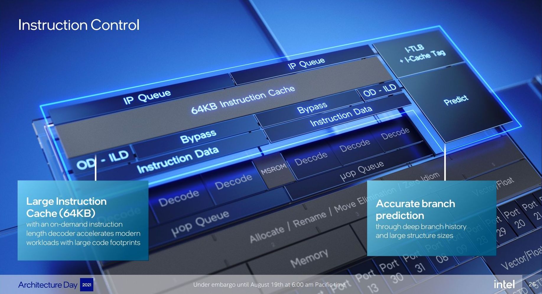
Back on the decoder, Intel supports on-demand decode which stores a history of previous decodes in the instruction cache and if recent misses are recalled at the decode stage, the on-demand stream will pull directly from the instruction cache instead, saving time – if the prefetch/decode works, the content in the instruction cache is updated, however if it is doing poorly then the scope is ‘re-enabled for general fetches’ to get a better understanding of the instruction flow. This almost sounds like a micro-op cache without having a physical cache, but is more to do about instruction streaming. Either way, the decoders can push up to six uops into the second half of the front end.
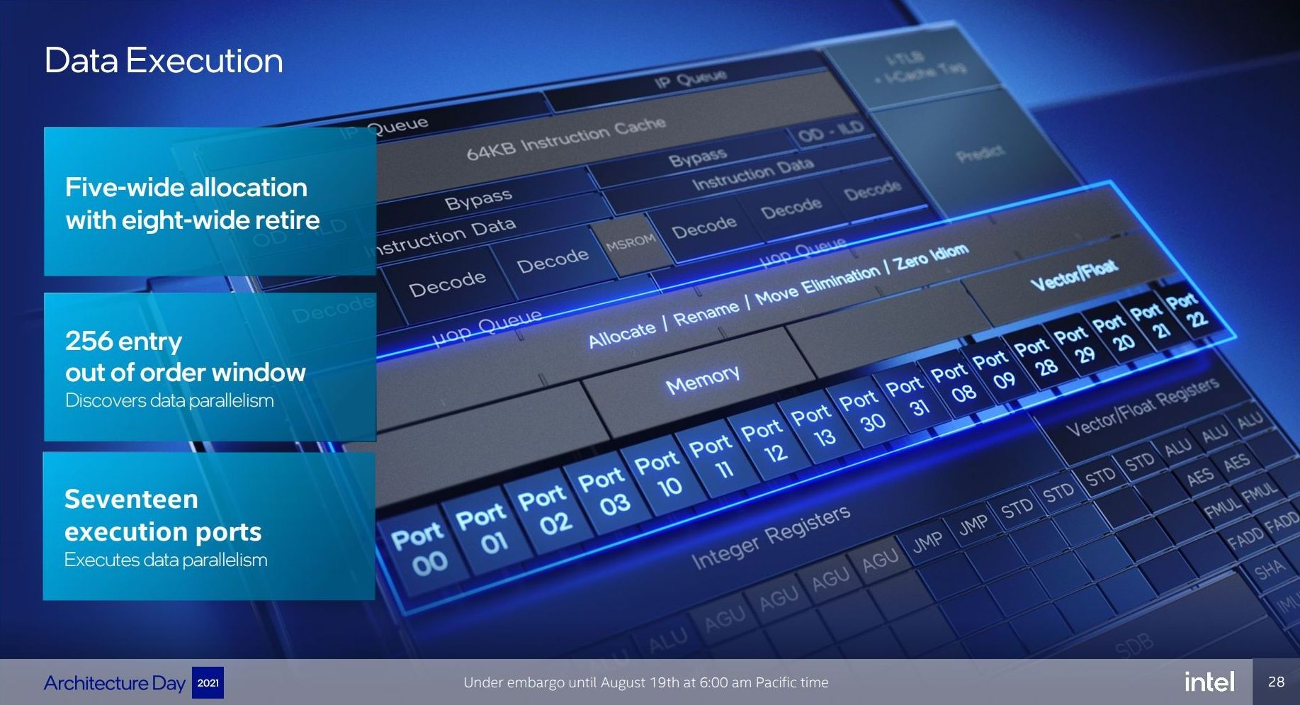
For Gracemont, the reorder buffer size has increased from 208 in Tremont to 256, which is important aspect given that Gracemont now has a total of 17 (!) execution ports, compared to eight in Tremont. This is also significantly wider than the execution capabilities of Golden Cove's 12 ports, related to the disaggregated integer and FP/vector pipeline design. However, despite that width, the allocation stage feeding into the reservation stations can only process five instructions per cycle. On the return path, each core can retire eight instructions per cycle.
Back End
So it’s a bit insane to have 17 execution ports here. There are a lot of repeated units as well, which means that Gracemont is expecting to see repeated instruction use and requires the parallelism to do more per cycle and then perhaps sit idle waiting for the next instructions to come down the pipe. Overall we have
- 4 Integer ALUs (ALU/Shift), two of which can do MUL/DIV
- 4 Address Generator Units, 2 Load + 2 Store
- 2 Branch Ports
- 2 Extra Integer Store ports
- 2 Floating Point/Vector store ports
- 3 Floating Point/Vector ALUs: 3x ALUs, 2x AES/FMUL/FADD, 1x SHA/IMUL/FDIV
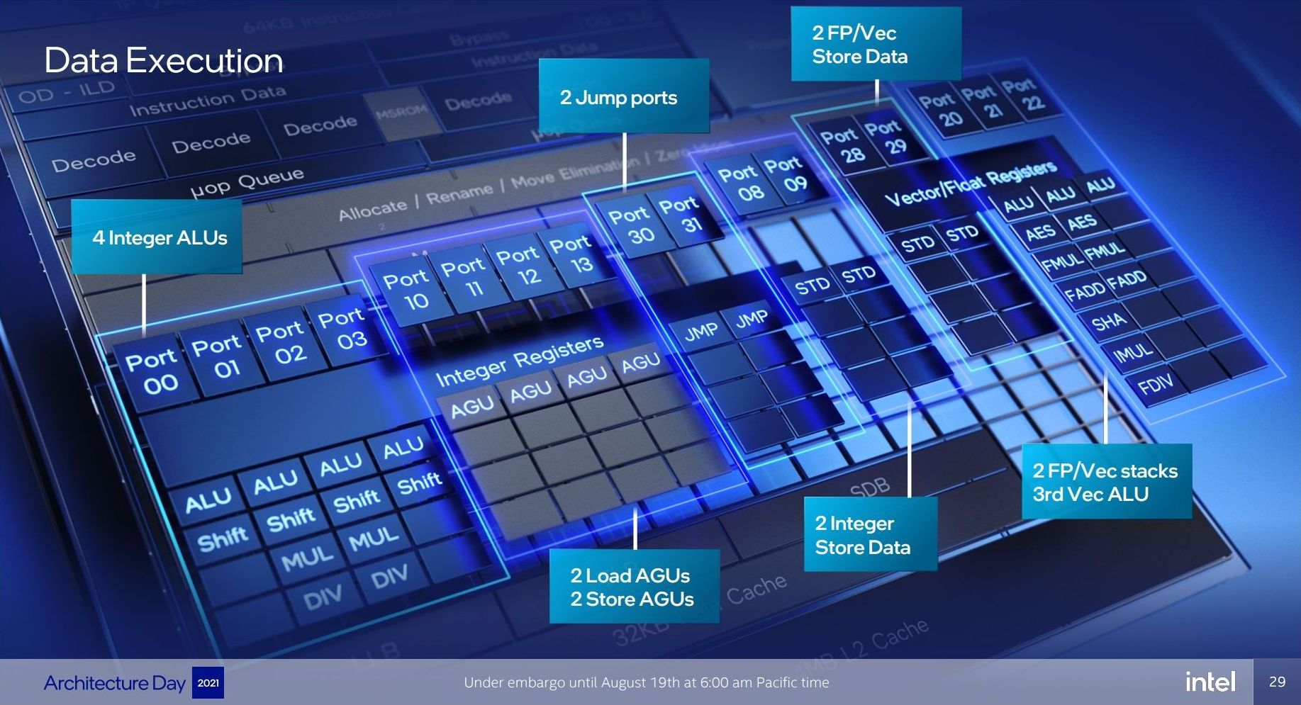
It will be interesting to see exactly how many of these can be accessed simultaneously. In previous core designs a lot of this functionality would be enabled though the same port – even Alder Lake’s P-core only has 12 execution ports, with some ports doing double duty on Vector and Integer workloads. In the P-core there is a single scheduler for both types of workloads, whereas in the E-core there are two separate schedulers, which is more akin to what we see on non-x86 core designs. It’s a tradeoff in complexity and ease-of-use.
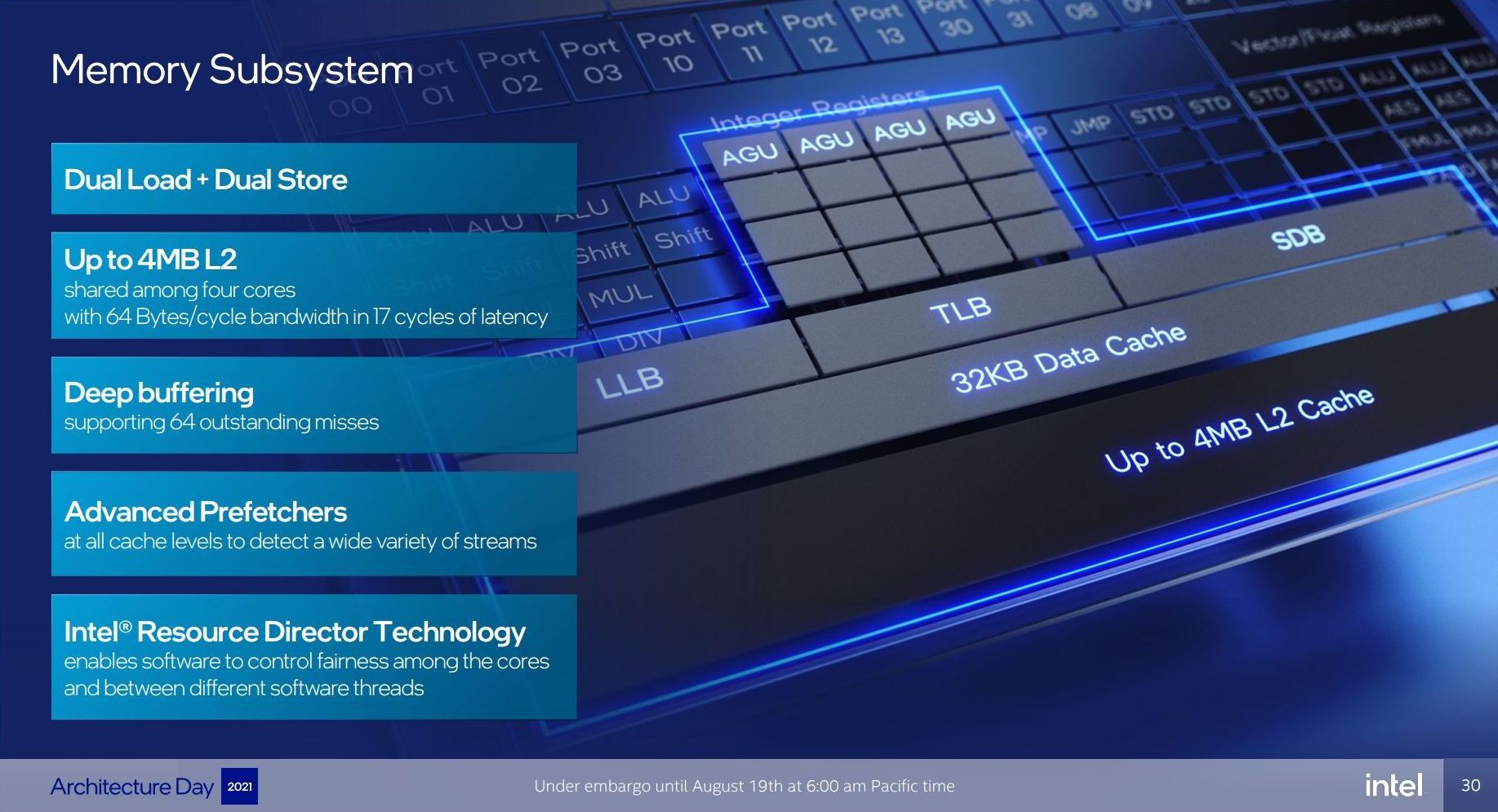
The back-end is support by a 32 KiB L1-Data cache, which supports a 3-cycle pointer chasing latency and 64 outstanding cache misses. There are two load and two store ports, which means 2x16 byte loads and 2 x 16 byte stores to the L1-D.
There is also has a shared 4 MB L2 cache across all four E-cores in a cluster with 17-cycle latency. The shared L2 cache can support 64 bytes per cycle read/write per core, which Intel states is sufficient for all four cores. The new L2 supports up to 64 outstanding misses to the deeper memory subsystem – which seems fair, but has to be shared amongst the 4 cores.
Intel states that it has a Resource Director that will arbitrate cache accesses between the four cores in a cluster to ensure fairness, confirming that Intel are building these E-cores in for multi-threaded performance rather than latency sensitive scenarios where one thread might have priority.
Other Highlights
As the first Atom core to have AVX2 enabled, there are two vector ports that support FMUL and FADD (port 20 and port 21), which means that we should expect peak performance compared to previous Atoms to be substantial. The addition of VNNI-INT8 over the AVX unit means that Intel wants these E-cores to enable situations where high inference throughput is needed, such as perhaps video analysis.
Intel was keen to point out that Gracemont has all of its latest security features including Control Flow Enhancement Technology (CET), and virtualization redirects under its VT-rp feature.
Overall, Intel stated that the E-cores are tuned for voltage more than anything else (such as performance, area). This means that the E-cores are set to use a lot less power, which may help in mobile scenarios. But as mentioned before on the first page, it will depend on how much power the ring has to consume in that environment - it should be worth noting that each four core Atom cluster only has a single stop on the full ring in Alder Lake, which Intel says should not cause congestion but it is a possibility – if each core is fully loaded, there is only 512 KB of L2 cache per core before making the jump to main memory, which indicates that in a fully loaded scenario, that might be a bottleneck.


223 Comments
View All Comments
name99 - Saturday, August 21, 2021 - link
As always the devil is in the details :-)Basic loop buffers, as in the LSD (introduced one gen before Nehalem, with Core2) have been with us forever, including early ARM chips and the early PA Semi chips, going on to Apple Swift.
But the basic loop buffer can not deal with branches (because part of the system is to switch off branch prediction!). Part of what makes the Apple scheme interesting and exceptional is that it's this graduated scheme that manages to extract much of the energy win from the repetition of loops while being able to cover a much wider variety of loops including those with (not too awful) patterns of function calls and branches.
Comparing details is usually unhelpful because different architectures have different concerns; obviously x86 has decode+variable length concerns which is probably THE prime concern for how their structure their attempts to extract performance and energy savings from loops,
On the Apple side, I would guess that Mapping (specifically detecting dependencies within a Decode group of 8 instructions, ie what register written by instruction A is immediately read by successor instruction B) is a high-energy task, and a future direction for all these loop techniques on the Apple side might be to somehow save these inter-instruction-dependencies in the loop storage structure? This is, obviously, somewhat different from Intel or AMD's prime concern with their loops, given that even now they max out at only 5 (perhaps soon 6) wide in the mapping stage, and don't need to know as much for mapping because they don't do as much zero-cycle work in the stage right after Mapping.
GeoffreyA - Sunday, August 22, 2021 - link
Thanks. I suppose storing the dependancy information would be of use even in non-loop cases, because of the amount of work it takes. Then again, it might add greater complexity, which is always a drawback.mode_13h - Sunday, August 22, 2021 - link
> I would guess that Mapping (specifically detecting ... what register written by> instruction A is immediately read by successor instruction B) is a high-energy task
So, do you foresee some future ISA trying to map these out at compile-time, like Intel's ill-fated EPIC tried to do? On the one hand, it bloats the instruction size with redundant information. On the other, it would save some expensive lookups, at runtime. I guess you could boil it down to a question of whether it takes more energy for those bits to come in from DRAM and traverse the cache hierarchy vs. doing more work inside the core.
The other idea I have is that if the CPU stores some supplemental information in its i-cache, then why not actually flush that out to L3 & DRAM, rather than recompute it each time? The OS would obviously have to provide the CPU with a private data area, sort of like a shadow code segment, but at least the ISA wouldn't have to change.
mode_13h - Saturday, August 21, 2021 - link
Thanks. Very nice incremental explanation of a loop buffer, trace cache, and L0.> n-way set-associative cache means you now have, n slots associated with a given index.
> So if you have 8 slots, you can hold 8 lines with that same index,
> ie 8 addresses with those same middle bits.
> BUT how do you know WHICH of those 8 lines you want?
Yeah, I know how a set-associative cache works. The simplistic explanation is that there's a n-entry CAM (Content-Addressable Memory) which holds the upper bits of the addresses (I think what you're calling Tags) for each cache line in a set. So, a cache lookup involves up to n (I suppose 8, in this case) comparisons against those upper bits, to find out if any of them match the requested address. And, ideally, we want the hardware to do all those comparisons in parallel, so it can give a quicker answer where our data is (or fetch it, if the cache doesn't have it).
Even at that level, cache is something not enough software developers know about. It's really easy to thrash a normal set-associative cache. Just create a 2D array with a width that's a factor or an integral multiple of a cache set size and do a column-traversal. If you're lucky, your entire array fits in L3. If not... :(
> which of these 8 possible lines is of interest is called a WAY.
Where I first learned about CPU caches, they called it a set. So, an 8-way set-associative cache had 8 sets.
> by storing the cache way, you can access a cache with the speed ...
> and energy ... of a direct-mapped cache.
Yup. That's what I thought you were saying. So, the way/set + offset is basically an absolute pointer into the cache. And a bonus is that it only needs as many bits as the cache size, rather than a full address. So, a 64k cache would need only 16 bits to uniquely address any content it holds.
GeoffreyA - Thursday, August 19, 2021 - link
I believe the reservation station is that portion which contains the scheduler and physical register files. In Intel, it's been unified since P6, compared to AMD's split/distributed scheduler design and, I think, Netburst.name99 - Thursday, August 19, 2021 - link
"Intel is noting that they’re doing an increased amount of dependency resolution at the allocation stage, actually eliminating instructions that otherwise would have to actually emitted to the back-end execution resources."Again presumably this means "executing" instructions at Rename (or earlier) rather than as actual execution.
Apple examples are
- handling some aspects of branches (for unconditional branches) at Decode
- zero cycle move. This means you treat a move from one register to another by creating a second reference to the underlying physical register. Sounds obvious, the trick is tracking how many references now exist to a given physical register and when it can be freed. It's tricky enough that Apple have gone through three very different schemes so far.
- zero cycle immediates. The way Apple handle this is a separate pool of ~40 integer registers dedicated to handling MOV xn, # (ie load xn with immediate value #), and the instruction is again handled to Rename.
Intel could do the same.They already do this for zero idioms, of course.
- then there are weirder cases like value prediction where again you insert the value into the target register at Rename. The instruction still has to be validated (hence executed in some form) but the early insertion improves. Apple does this for certain patterns of loads, but the details are too complicated for here.
mode_13h - Friday, August 20, 2021 - link
Thanks again!name99 - Thursday, August 19, 2021 - link
"Someone please remind us what a reservation station is?"After an instruction is decoded it passes through Rename where resources it will need later (like a destination register, or a load/store queue entry) are allocated.
Then it is placed in a Scheduling Queue. It sits in the queue until its dependencies are resolved (ie ADD x0, x1, x2 cannot execute until the values of x1 and x2 are known.
This Scheduling Queue is also called a Reservation Station.
There is a huge dichotomy in design here. Intel insists on using a single such queue, everyone else uses multiple queues. Apple have a queue per execution unit, ala https://twitter.com/dougallj/status/13739734787312... (this is not 100% correct, but good enough).
The problem with a large queue is meeting cycle time. The problem with multiple queues is that they can get unbalanced. It's sad if you are executing integer only code and can't use the FP queue slots. Even worse is if you have one of your integer queues totally full, and the others empty, so only that one queue dispatches work per cycle.
Apple solve these in a bunch of ways.
First note the Dispatch Buffer in front of the Queues. This accepts instructions up to 8-wide per cycle from Rename, and sends as many as possible to the Scheduling Queues. It engages in load balancing to make sure that queues are always as close to evenly filled as possible.
Secondly the most recent Apple designs pair the Scheduling Queues so that, ideally, each queue issues one instruction, but if a Queue cannot find a runnable instruction, it will accept the second choice runnable candidate from its paired queue.
Queues and scheduling are actually immensely complicated. You have hundreds of instructions, all of which could depend in principle on any earlier instruction, so how do track (at minimal area and energy) all these dependencies? Apple appears to use a Matrix Scheduler with a TRULY ASTONISHINGLY CLEVER dependency scheme. A lot about the M1 impresses me, but if I had to choose one thing it might be this.
It's way too complicated to describe here, but among the things you need to bear in mind are
- you want to track which instructions depend on which
- you want to track the age of instructions (so that when multiple instructions are runnable, earliest go first)
- you need to handle Replay. I won't describe this here, but for people who know what it is, Apple provide
+ cycle-accurate Replay (no randomly retrying every four cycles till you finally succeed!) AND, most amazingly
+ perfect DEMAND Replay (only the instructions, down a chain of dependencies) that depended on a Replay are in turn Replayed (and, again, at the cycle accurate time)
+ if you think that's not amazing enough, think about what this implies for value prediction, and how much more aggressive you can be if the cost of a mispredict is merely a cycle-accurate on-demand Replay rather than a Flush!!!
mode_13h - Friday, August 20, 2021 - link
Wow, you're on a roll!name99 - Thursday, August 19, 2021 - link
"> full-line-write predictive bandwidth optimisation ... where the core can greatly improve> bandwidth by avoiding RFO reads of cache lines that are going to be fully rewritten"
Of course this is one of those "about time" optimizations :-)
Apple (it's SO MUCH EASIER with a decent memory model, so I am sure also ARM) have had this for years of course. But improvements to it include
- treat all-zero lines as special cases that are tagged in L2/SLC but don't require transferring data on the NoC. Intel had something like this in IceLake that, after some time, they switched off with microcode update.
- store aggregation is obvious and easy if your memory model allows it. But Apple also engages in load aggregation (up to a cache line width) for uncachable data. I'm not sure what the use cases of this are (what's still uncachable in a modern design? reads rather than DMA from PCIe?) but apparently uncachable loads and stores remain a live issue; Apple is still generating patents about them even now.
- Apple caches all have a bit per line that indicates whether this line should be treated as streaming vs LRU. Obviously any design that provides non-temporal loads/stores needs something like that, but the Apple scheme also allows you to mark pages (or range registers, which are basically BATs -- yes PPC BATs are back, baby!) as LRU or streaming, then the system will just do the right thing whether that data is accessed by load/stores, prefetch or whatever else.
BTW, just as an aside, Apple's prefetchers start at the load-store unit, not the L1. Meaning they see the VIRTUAL address stream.) This in turn means they can cross page boundaries (and prefetch TLB entries for those boundary crossings). They're also co-ordinated so that each L1 is puppeting what it want the L2 prefetcher to do for it, rather than having L1 and L2 prefetchers working independently and hoping that it kinda sorta results in what you want. And yes, of course, tracking prefetching efficiency and throttling when appropriate have always been there.