IBM Creates First 2nm Chip
by Dr. Ian Cutress on May 6, 2021 6:00 AM EST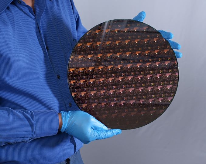
Every decade is the decade that tests the limits of Moore’s Law, and this decade is no different. With the arrival of Extreme Ultra Violet (EUV) technology, the intricacies of multipatterning techniques developed on previous technology nodes can now be applied with the finer resolution that EUV provides. That, along with other more technical improvements, can lead to a decrease in transistor size, enabling the future of semiconductors. To that end, Today IBM is announcing it has created the world’s first 2 nanometer node chip.
Names for Nodes
Just to clarify here, while the process node is being called ‘2 nanometer’, nothing about transistor dimensions resembles a traditional expectation of what 2nm might be. In the past, the dimension used to be an equivalent metric for 2D feature size on the chip, such as 90nm, 65nm, and 40nm. However with the advent of 3D transistor design with FinFETs and others, the process node name is now an interpretation of an ‘equivalent 2D transistor’ design.
Some of the features on this chip are likely to be low single digits in actual nanometers, such as transistor fin leakage protection layers, but it’s important to note the disconnect in how process nodes are currently named. Often the argument pivots to transistor density as a more accurate metric, and this is something that IBM is sharing with us.
Transistor Density
Today’s announcement states that IBM’s 2nm development will improve performance by 45% at the same power, or 75% energy at the same performance, compared to modern 7nm processors. IBM is keen to point out that it was the first research institution to demonstrate 7nm in 2015 and 5nm in 2017, the latter of which upgraded from FinFETs to nanosheet technologies that allow for a greater customization of the voltage characteristics of individual transistors.
IBM states that the technology can fit ’50 billion transistors onto a chip the size of a fingernail’. We reached out to IBM to ask for clarification on what the size of a fingernail was, given that internally we were coming up with numbers from 50 square millimeters to 250 square millimeters. IBM’s press relations stated that a fingernail in this context is 150 square millimeters. That puts IBM’s transistor density at 333 million transistors per square millimeter (MTr/mm2).
For comparison:
| Peak Quoted Transistor Densities (MTr/mm2) | ||||
| AnandTech | IBM | TSMC | Intel | Samsung |
| 22nm | 16.50 | |||
| 16nm/14nm | 28.88 | 44.67 | 33.32 | |
| 10nm | 52.51 | 100.76 | 51.82 | |
| 7nm | 91.20 | 237.18* | 95.08 | |
| 5nm | 171.30 | |||
| 3nm | 292.21* | |||
| 2nm | 333.33 | |||
| Data from Wikichip, Different Fabs may have different counting methodologies * Estimated Logic Density |
||||
As you can tell, different foundries have different official names with a variety of densities. It’s worth noting that these density numbers are often listed as peak densities, for transistor libraries where die area is the peak concern, rather than frequency scaling – often the fastest parts of a processor are half as dense as these numbers due to power and thermal concerns.
Stacked GAA
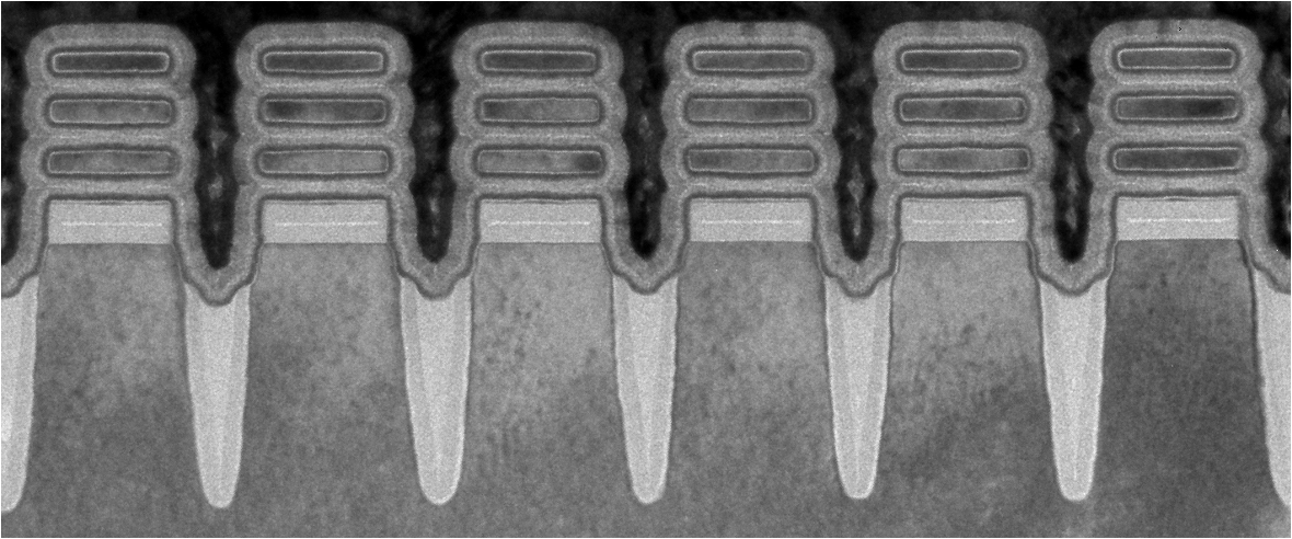
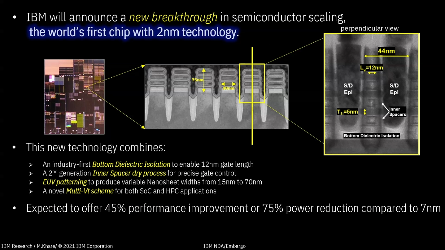
With regards the movement to Gate-All-Around / nanosheet transistors, while not explicitly stated by IBM, images show that this new 2nm processor is using a three-stack GAA design. Samsung is introducing GAA at 3nm, while TSMC is waiting until 2nm. Intel by contrast, we believe, will introduce some form of GAA on its 5nm process.
IBM’s 3-stack GAA uses a cell height of 75 nm, a cell width of 40 nm, and the individual nanosheets are 5nm in height, separated from each other by 5 nm. The gate poly pitch is 44nm, and the gate length is 12 nm. IBM says that its design is the first to use bottom dieletric isolation channels, which enables the 12 nm gate length, and that its inner spacers are a second generation dry process design that help enable nanosheet development. This is complimented by the first use of EUV patterning on the FEOL parts of the process, enabling EUV at all stages of the design for critical layers.
Users might be wondering why we’re hearing that IBM is the first to a 2nm chip. IBM is one of the world’s leading research centers on future semiconductor technology, and despite not having a foundry offering of their own, IBM develops IP in collaboration with others for their manufacturing facilities. IBM sold its manufacturing to GlobalFoundries with a 10 year partnership commitment back in 2014, and IBM also currently works with Samsung, and recently announced a partnership with Intel. No doubt the latter two will be partnering with IBM on some level around this new development for its viability in their own production chain.
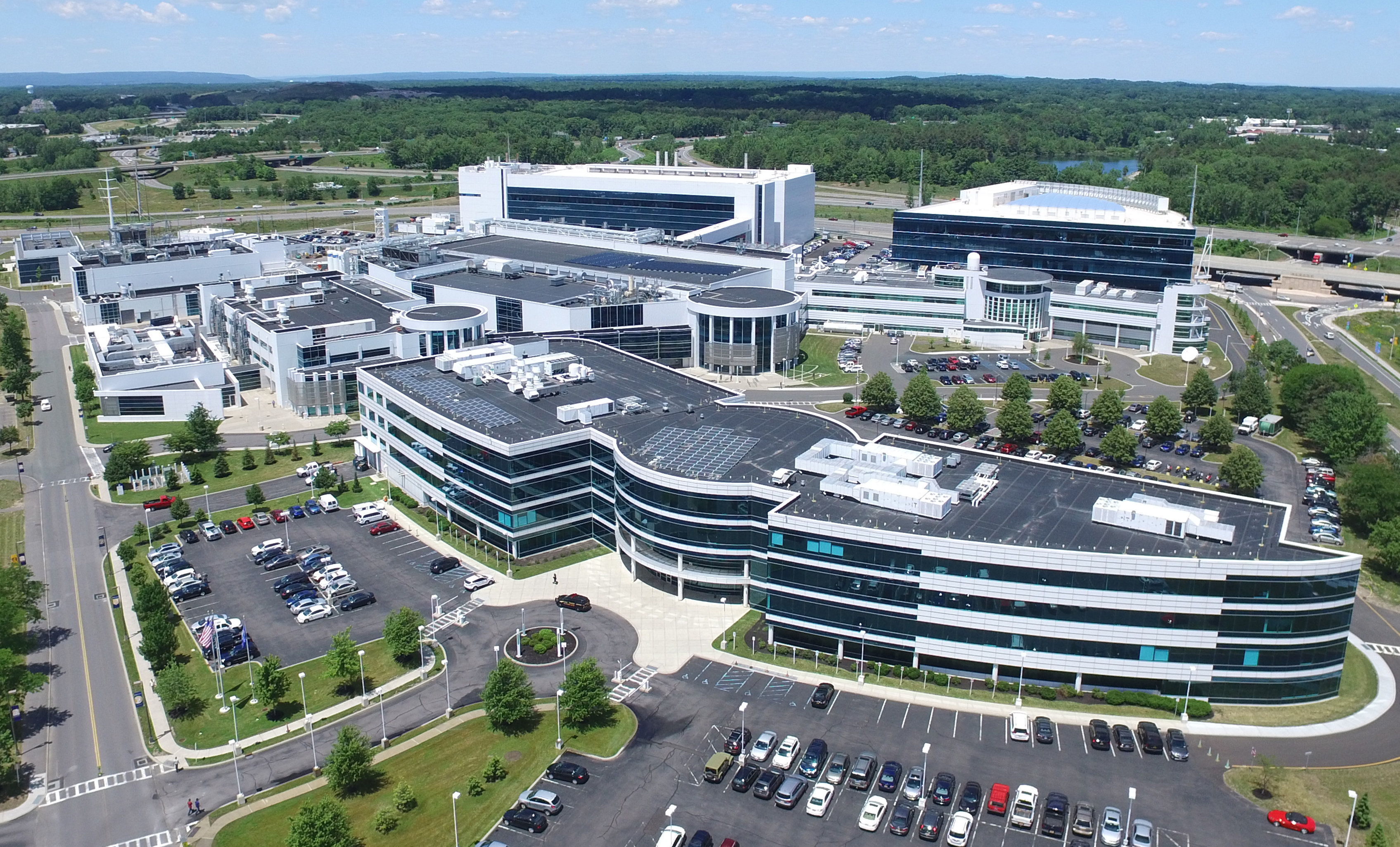
IBM Albany Research Center
No details on the 2nm test chip have been provided, although at this stage it is likely to be a simplified SRAM test vehicle with a little logic. The 12-inch wafer images showcase a variety of different light diffractions, which likely points to a variety of test cases to affirm the viability of the technology. IBM says that the test design uses a multi-Vt scheme for high-performance and high-efficiency application demonstrations.

Wafer up close
The chip was designed and made at IBM’s Albany research facility, which features a 100,000 sq. ft. clean room. The purpose of this facility is to build on IBM’s expansive patent and licensing portfolio for collaborations with partners.
We have a set of questions with IBM’s experts awaiting response. We also now have an active invitation to go visit, as and when we can travel again.
Related Reading
- IBM and AMD to Advance Confidential Computing
- Hot Chips 2020 Live Blog: IBM z15, a 5.2 GHz Mainframe CPU (11:00am PT)
- IBM & Partners to Fight COVID-19 with Supercomputers, Forms COVID-19 HPC Consortium
- Hot Chips 31 Live Blogs: IBM's Next Generation POWER
- IBM to use Samsung 7nm EUV for Next-Gen POWER and z CPUs
- IBM And Everspin Announce 19TB NVMe SSD With MRAM Write Cache
- TSMC Update: 2nm in Development, 3nm and 4nm on Track for 2022
- Intel’s Manufacturing Roadmap from 2019 to 2029: Back Porting, 7nm, 5nm, 3nm, 2nm, and 1.4 nm


118 Comments
View All Comments
FreckledTrout - Thursday, May 6, 2021 - link
Oh it is very impressive. That however was part of the issue scaling to high power chips. Intel simply pushed things to far. They have had to loosen those densities up for high power 10nm chips and introduce some extra tricks like SuperFin.movax2 - Thursday, May 6, 2021 - link
Yeah, intel 10nm++(+) is so impressive than even Rocket-Lake was still 14nm+++++.And Alder-Lake 10nm+++(+) will still have 8 big cores comparing to Zen3 16 cores.
Yeah , very "impressive"
name99 - Thursday, May 6, 2021 - link
Impressive --- and irrelevant. Intel does not make any device even CLOSE to those limits. Which makes you wonder WTF they bothered to try to reach them.The best they hit right now is ~50MTr/mm^2
https://www.anandtech.com/show/15877/intel-hybrid-...
Will Xe be better? Who knows? The rough guesses we can make from the iGPUs on existing Intel chips certainly don't suggest that Intel's GPUs run at substantially higher density that the CPUs.
So -- kill your process so you can boast of >100MTr/mm^2 -- then ship devices that only exploit half that value? Still unclear to me quite what the strategy behind that is...
(FWIW for 7nm we have multiple vendors confirming then hit >90% of TSMC's promised density.
For 5nm the situation is unclear.
- The Apple results are (IMHO) meaningless because A14/M1 were clearly rushed in the sense that the ONLY priority was getting the x86/mac stuff working. The core that's not relevant to that is barely altered, the GPU is barely altered. I don't expect much effort at all was put into physical optimization. I don't think we'll have "reasonable" Apple results till at least the A15/M2.
- Huawei only produced a few chips on 5nm before US Govt forced them off the process. I have seen lots of claims about the Huawei density, but they all strike me as BS, as repeating the baseline TSMC 5nm density. Not a single independent measurement or something equivalent.
- We have no QC or anyone else on TSMC 5nm yet
So if someone tells you they know what achievable TSMC 5nm density is [or associated results, like the claim of *substantially* worse SRAM scaling] treat them as charlatans. So far this info is simply not public; all that is public is a lot of loud voices and ill-informed speculation.)
Spunjji - Friday, May 7, 2021 - link
I will probably die mad about the constant quoting of the 100MTr/mm^2 number 😅Kuhar - Friday, May 7, 2021 - link
It is impressive indeed but i guess you missed the word "peak" in the article. It is the peak density and quite nicely explained what it means.FunBunny2 - Thursday, May 6, 2021 - link
of most interest: how much of the production machinery is bespoke by IBM? or do they use the same ASML, et al commodity machines? IOW, is IBM really all that far ahead of the curve?Arsenica - Thursday, May 6, 2021 - link
They use pretty much the same equipment as everyone else.For EUV the Albany campus had one-off machines like a custom Micro Exposure Tool and the first Alpha Demo Tool from ASML, but right now they are using the NXE3400 from ASML.
The smallest X-Y dimension here is the 12 nm gate-length that was likely made using the NXE3400's 13 nm resolution plus some "resolution enhancement" via etching
forextor - Thursday, May 6, 2021 - link
I wonder how small my 1.44" floppy disk drive would be (or how much data can it hold) if it is using this technology.Tomatotech - Thursday, May 6, 2021 - link
"Smaller than your fingernail ..."Spunjji - Friday, May 7, 2021 - link
You can currently get 1TB Micro SD cards that are a similar size to most people's fingernails. That's a more valid comparison - this process couldn't be used to make non-volatile storage,