Intel Teases Ponte Vecchio Xe-HPC Power On, Posts Photo of Server Chip
by Ryan Smith on January 26, 2021 11:40 AM EST- Posted in
- GPUs
- Intel
- Xe
- Ponte Vecchio
- Xe-HPC
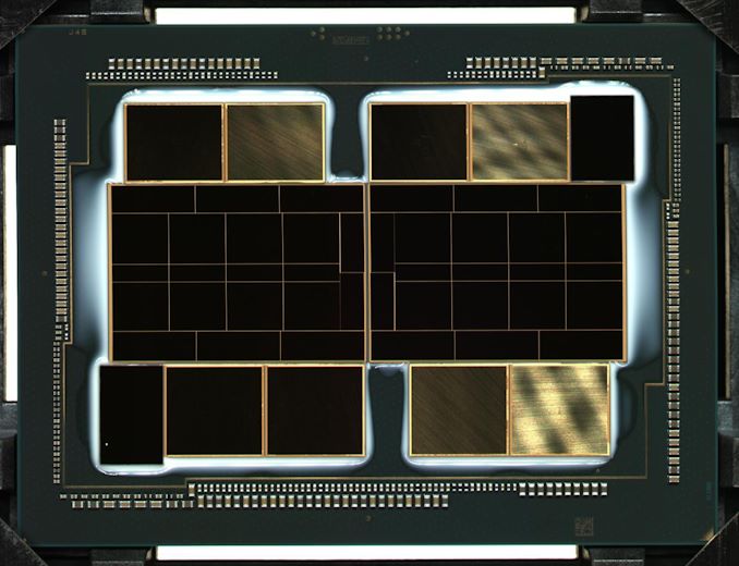
In what’s turning into an Xe sort of day, Intel’s GPU guru and frontman for their GPU division, Raja Koduri, has tweeted that the company is getting ready to begin power on testing for their forthcoming high-end server GPU, the Xe-HPC based Ponte Vecchio. And along with this announcement, Koduri has also posted a somewhat redacted photo of the sizable chip.
Xe HPC ready for power on!
— Raja Koduri (@Rajaontheedge) January 26, 2021
7 advanced silicon technologies in a single package
Silicon engineers dream
Thing of beauty @intel pic.twitter.com/RF8Prsy05f
According to Koduri, Ponte Vecchio incorporates “7 advanced silicon technologies,” likely referring to everything from the four different process nodes used to make the chiplets, to memory stacks, and including the Foveros packaging.
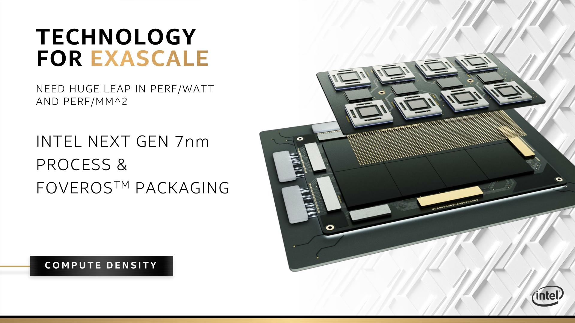
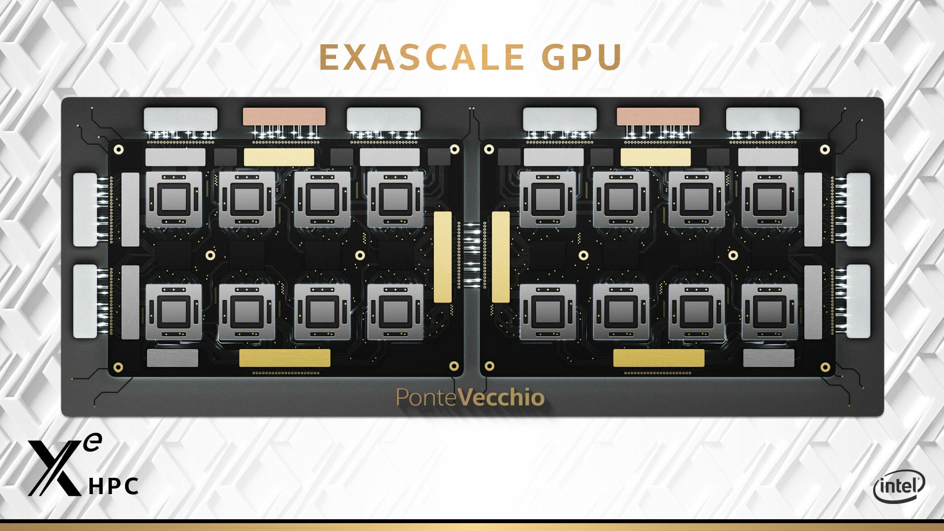
Ponte Vecchio is a keystone project for Intel’s GPU division. Along with being the largest and grandest of their Xe GPUs, the chip will be at the heart of the Aurora supercomputer, Intel’s most recent supercomputer win. So a lot is riding on the chip, and no doubt Intel’s engineers are eager to see a successful power-on test.
Source: Raja Koduri (Twitter)


31 Comments
View All Comments
shabby - Tuesday, January 26, 2021 - link
7nm + 7 advanced silicon technologies... the yield rate must be in the single digits no?Ian Cutress - Tuesday, January 26, 2021 - link
Each one of the small die can be binned for yield, so when you're doing advanced packaging, you know that everything coming together is using known good die (KGD). Then it's a factor of the packaging yield process.FunBunny2 - Tuesday, January 26, 2021 - link
"Each one of the small die can be binned for yield, so when you're doing advanced packaging, you know that everything coming together is using known good die (KGD). "may be they could/should bin the Big Banks into banklets?
bananaforscale - Wednesday, January 27, 2021 - link
7%?JayNor - Tuesday, January 26, 2021 - link
That's some amazingly tight stitching. I was expecting something more spread out, similar to the proportions of Raja's slide presentations.JayNor - Wednesday, February 10, 2021 - link
Looks like all those internal chiplets are stacked on top of seven XEMF chiplets in a foveros stacking, rather than being stitched together by emib.brucethemoose - Tuesday, January 26, 2021 - link
So... 8 HBM stacks. 2 IO dies? Possibly a bunch of separate compute and cache tiles?*Whistles* that's quite a package.
brucethemoose - Tuesday, January 26, 2021 - link
*Now I realize thats probably 2 big single dies in the middle.edzieba - Tuesday, January 26, 2021 - link
The two big dies are using Foveros, so two large 'lower' dies with that patchwork of 'upper' dies above them, then EMIB underneath that to connect to the HBM stacks on the periphery and the link I/O tiles, as well as another EMIB bridge or two between the two Foveros stacks.Exotica - Tuesday, January 26, 2021 - link
Can someone in layman’s terms describe a power on test and its purpose, as well as where it falls in the chip design process ? When the chip comes out of the fab, hasn’t it already been powered on? Just trying to understand. Thanks.