Intel’s 11th Gen Core Rocket Lake Detailed: Ice Lake Core with Xe Graphics
by Dr. Ian Cutress on October 29, 2020 11:00 AM EST- Posted in
- CPUs
- Intel
- 14nm
- Xe-LP
- 11th Gen
- Rocket Lake
- Cypress Cove
During a time of increased competitor activity, Intel has decided to disclose some of the high level details surrounding its next generation consumer processor, known as Rocket Lake or Intel’s 11th Gen Core. The new processor family is due in the market in the first quarter of 2021, and is expected to share a socket and motherboard compatibility with the current 10th Gen Comet Lake processors, providing an upgrade path even for those with a Core i9-10900K, Intel’s highest performing desktop processor to date. New 500-series motherboards are also expected to be available.
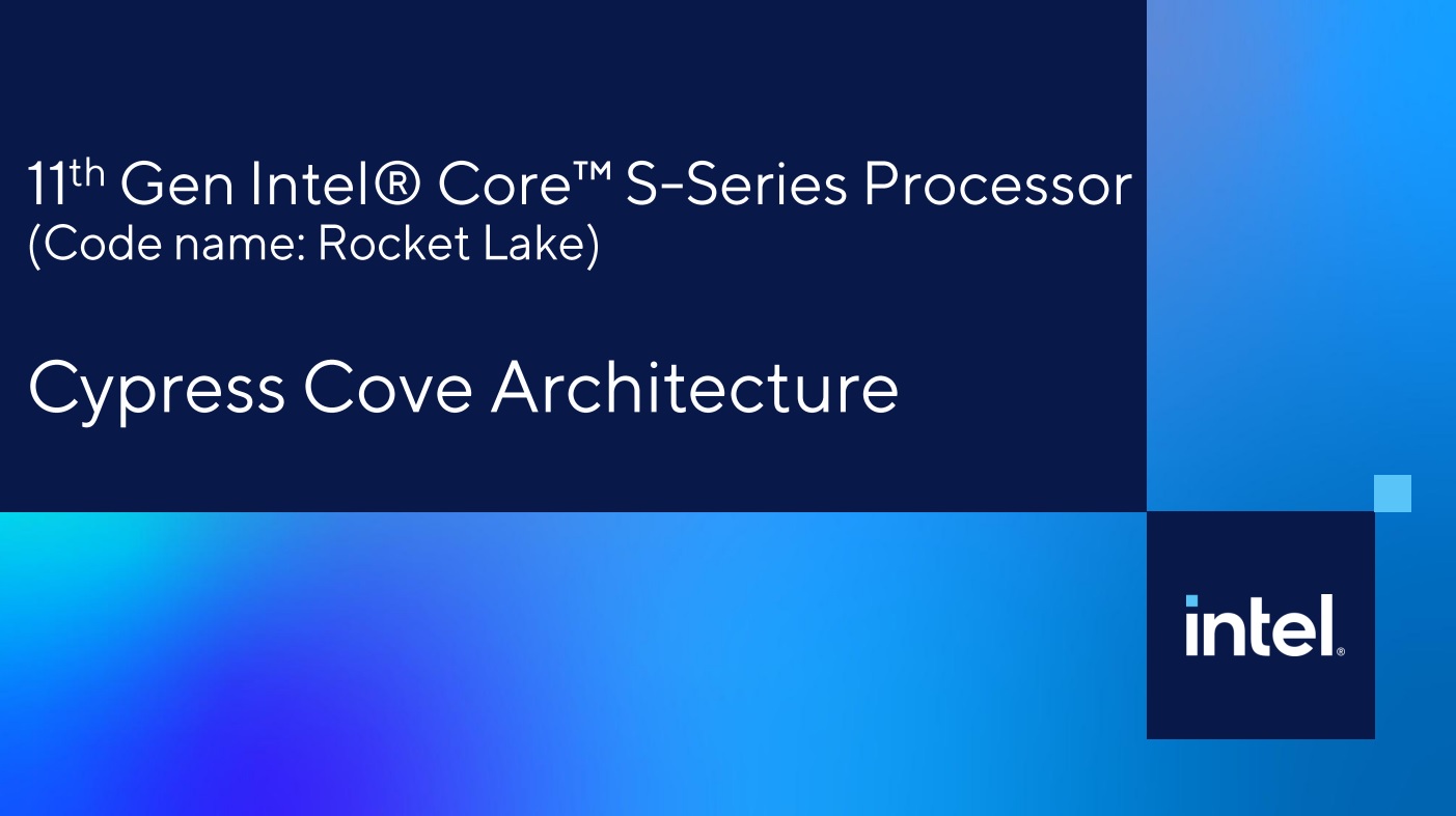
The new Rocket Lake-S silicon or SoC is going to be known as ‘Cypress Cove’. Intel confuses itself in the press release compared to the PDF presentation, as the press release dictates that this isn’t the core – it specifically states that the core microarchitecture is Ice Lake (Sunny Cove). However the presentation PDF says Cypress Cove is the core. In this instance, to be clear, Sunny Cove and Cypress Cove are set to be practically identical, however Sunny Cove is on 10nm and Cypress Cove is the back-ported variant on 14nm.
Paired with these cores will be the Tiger Lake graphics architecture, known as Xe-LP, which is also being backported from 10nm to 14nm for this product. The combined 14nm representation of Ice Lake cores and Xe-LP graphics is what is going to be known as Rocket Lake, (at least one of) the SoC(s) of the 11th Gen Core family.
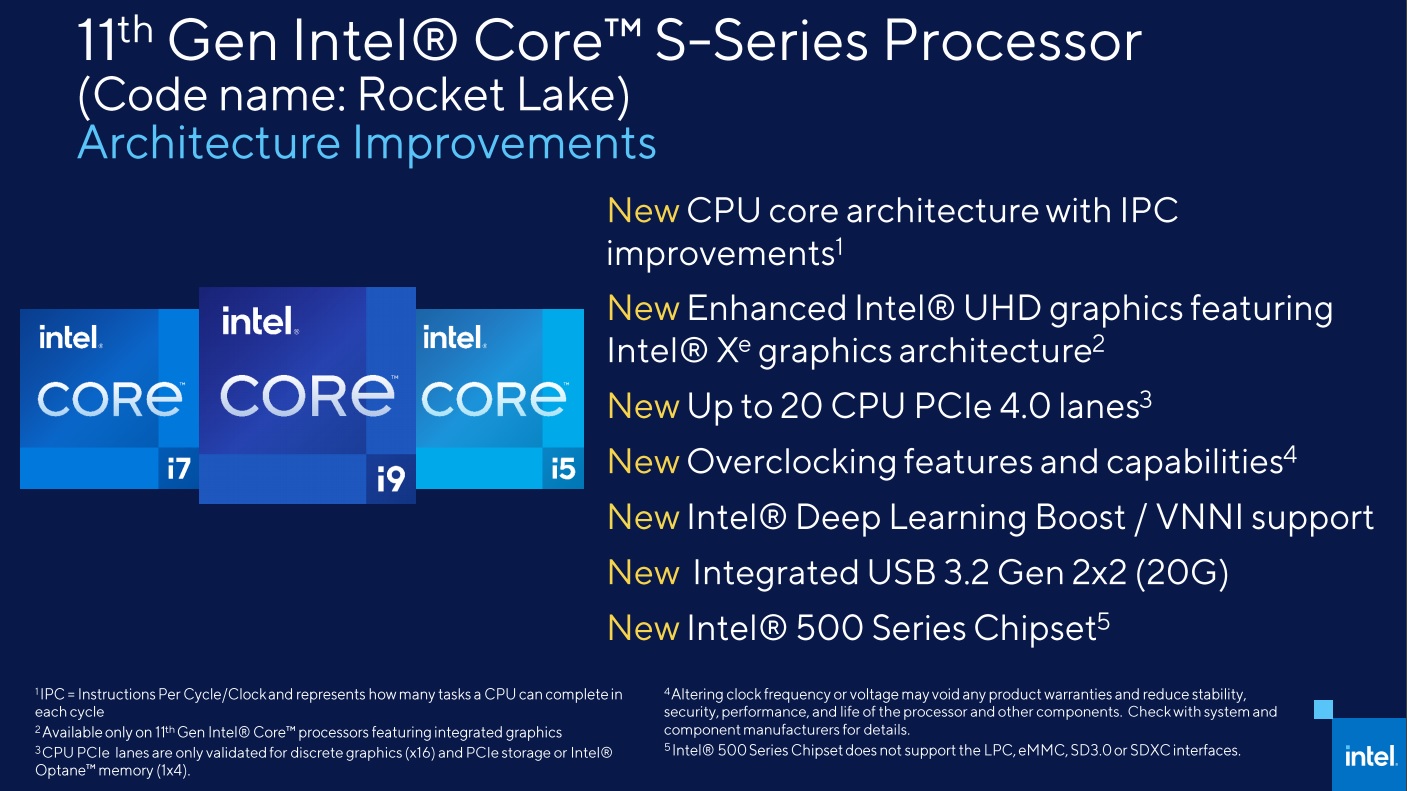
With the new processors, Intel is targeting a raw instruction-per-clock uplift in the double digit range, which would be similar to the uplift we saw moving from Comet Lake to Intel’s Ice Lake mobile processors. Because of the node difference, the exact IPC change is likely to be lower than what we’ve seen before, but 10%+ is still highly respectable, especially if Intel is also able to maintain the high frequency it has achieved with the current generation of Comet Lake.
One of the benefits of moving to a back-ported Sunny Cove core will be the inclusion of the AVX-512 vector acceleration unit in Cypress Cove. This enables Intel to enable its library of Deep Learning Boost technologies for AI and ML acceleration, including support for Vector Neural Network Instructions (VNNI), finally bringing AVX-512 to the desktop platform.
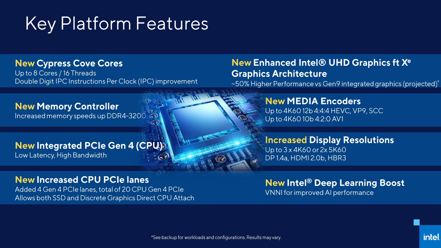
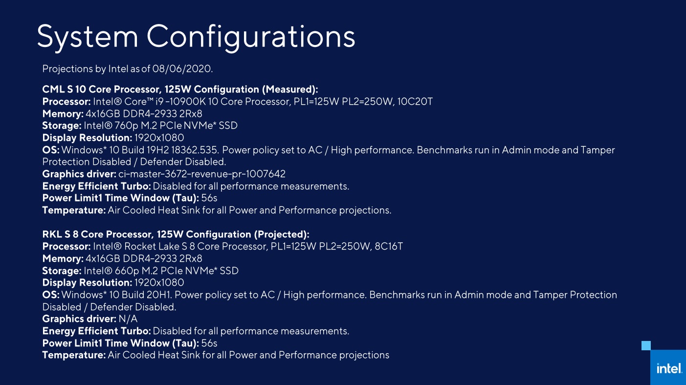
However, to mix and match the right combination of core count, graphics, and AVX-512 for die size/yield/cost, it appears that Rocket Lake-S will only offer a maximum of eight cores in its largest configuration. Within the press release PDF, Intel stated that the current silicon as tested is rated for 125 W TDP, with a top turbo boost of 250 W, which matches what we see on the Core i9-10900K already. There’s no escaping the performance-per-watt characteristics of the process node, which indicates that Intel might find hitting those high frequencies a little easier with fewer cores to deal with. Intel is also promoting new overclocking tools with Rocket Lake, however did not go into details.
Another feature that Intel has disclosed with Rocket Lake is the move to PCIe Gen 4.0 on the processor, with up to 20 lanes available. These are likely to be split into one x16 for graphics and one x4 for storage on most motherboards, and this aligns with what we’ve seen on the latest generation of Intel Z490 motherboards, some of which have already promoted support for PCIe 4.0 ‘on future Intel processors’. This means Rocket Lake. Intel also mentions that the memory controller now supports up to DDR4-3200, however the projected performance numbers were done with DDR4-2933 memory.
On the graphics side, moving to the Xe-LP graphics architecture is going to be a big uplift in graphics performance, with Intel suggesting a 50% improvement over current Comet Lake integrated graphics. It is worth noting here in the slide that Intel mentions ‘UHD Graphics ft Xe Graphics Architecture’ – this would perhaps point to a scaled down version of Xe compared to Tiger Lake. I’m fully expecting to see only 32 EUs here, as a balance between die area, power, and performance. In the fine print it suggests that there will be some versions of Rocket Lake without the integrated graphics enabled, similar to the F processors we see on the market today.
That being said, for those units with integrated graphics, Intel is promoting new media encoders and display resolution support, with up to 4K60 12-bit for 4:4:4 HEVC and VP9, or up to 4K60 with 10-bit 4:2:0 AV1, showcasing AV1 support for mainstream processors. Display resolution support has also increased, with up to three 4K60 displays or two 5K60 displays, supporting DP 1.4a (with HBR3) and HDMI 2.0b.
This was an unexpected news announcement this morning - speaking to peers it all seems to be a bit of a surprise - perhaps even for the PR teams, given that the system configurations as 'projected' in the slide above is dated 6th August, almost 3 months ago. It will be interesting to hear if Intel will disclose more details ahead of launch.
Source: Intel
Related Reading
- Intel Confirms Rocket Lake on Desktop for Q1 2021, with PCIe 4.0
- The Intel Comet Lake Core i9-10900K, i7-10700K, i5-10600K CPU Review
- The Intel Core i7-8086K Review


188 Comments
View All Comments
colinisation - Thursday, October 29, 2020 - link
Why are they bringing AVX-512 to the mainstream desktop? Is it confirmed to be full fat 512bit vector processing, or will the be split into 2, 256 bit chunks like zen 1 and 256 bit AVX? Not a software dev but I think full fat 512 bit is a waste on the home desktop.Does this core support TSX, does TSX have a future in Intel CPU's?
SarahKerrigan - Thursday, October 29, 2020 - link
On laptops, which use the same core, it's full-on AVX-512.IntelUser2000 - Thursday, October 29, 2020 - link
Nope.Icelake and Tigerlake is 512 split into two.
SarahKerrigan - Thursday, October 29, 2020 - link
Is it? I thought that was only true of load/store ops. Definitely willing to learn something, though - my only AVX512 exposure has been on SKL-SP (where the app got solid performance wins over the previous AVX2 implementation.)saratoga4 - Thursday, October 29, 2020 - link
Icelake has full 512 bit wide vector units and data paths, so not split in two. Probably he is confusing Icelake (1x512 wide) with Skylake-SP(2x512 wide). So yes, it is half (512 bit) of the previous Skylake-SP (1024 bit).Elstar - Friday, October 30, 2020 - link
It's more complicated than that. For example, see this diagram:https://en.wikichip.org/wiki/intel/microarchitectu...
Basically, Skylake-SP has three execution units. Two are 256-bit wide and one is 512-bit wide; and the smaller 256-bit units can be synchronized to execute AVX512 instructions.
The net effect is -- roughly speaking -- that one can either start executing three AVX2 instructions in a given cycle or two AVX512 instructions (because two of the units need to be ganged together).
What consumers are getting in Ice Lake and later is the ability for two 256-bit execution units to be lashed together to execute AVX512 instructions. I believe the dedicated 512-bit execution unit is sill server/workstation only.
Also, ganging together execution units is quite normal. When 128-bit SSE came out, those instructions were emulated via 64-bit execution units. And for a while, 256-bit AVX instructions were emulated via 128-bit execution units. In fact, it was only with Zen 2 that AMD started natively having 256-bit wide execution units, thus allowing some serious performance gains when executing AVX code.
dotjaz - Saturday, October 31, 2020 - link
ICL doesn't split, rather fuses 2x256 to 1x512. Not exactly the same but makes no real difference anyway.Kevin G - Thursday, October 29, 2020 - link
It didn't split, kinda. SkyLake SP has an extra true 512 bit wide unit. The consumer cores never got it.dotjaz - Saturday, October 31, 2020 - link
ICL uses 2x256bit FMA/Vec units to do one 512bit, Intel didn't explicitly say it, but it can only execute 1x512bit and not 1x512+1x256, what else can it be?Revdarian - Thursday, October 29, 2020 - link
The real problem with AVX-512 is "which actual feature set of AVX-512 is going to be present?" because unlike the other types of advanced vector extensions, there is not a one size standard but instead multiple different extensions and you aren't required, nor expected, to support them all in order to claim AVX-512 support, creating a bigger fragmentation than just "it has AVX-512 or not". This was a mistake on intel's part imho and is what soured Linus Torvald and other developers regarding the instructions.