HPC Systems Special Offer: Two A64FX Nodes in a 2U for $40k
by Dr. Ian Cutress on June 26, 2020 10:00 AM EST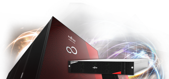
It was recently announced that the Fugaku supercomputer, located at Riken in Japan, has scored the #1 position on the TOP500 supercomputer list, as well as #1 positions in a number of key supercomputer benchmarks. At the heart of Fugaku isn’t any standard x86 processor, but one based on Arm – specifically, the A64FX 48+4-core processor, which uses Arm’s Scalable Vector Extensions (SVE) to enable high-throughput FP64 compute. At 435 PetaFLOPs and 7.3 million cores, Fugaku beat the former #1 system by 2.8x in performance. Currently Fugaku has been used for COVID-19 related research, such as modelling tracking rates or virus in liquid droplet dispersion.
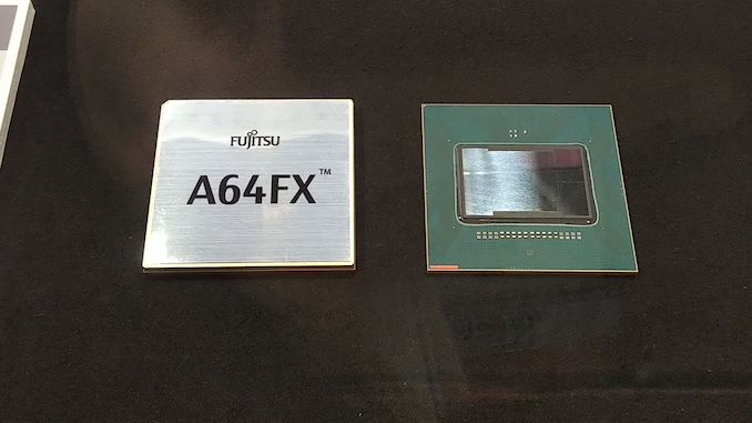
The Fujitsu A64FX card is a unique piece of kit, offering 48 compute cores and 4 control cores, each with monumental bandwidth to keep the 512-bit wide SVE units fed. The chip runs at 2.2 GHz, and can operate in FP64, FP32, FP16 and INT8 modes for a variety of AI applications. There is 1 TB/sec of bandwidth from the 32 GB of HBM2 on each card, and because there are four control cores per chip, it runs by itself without any external host/device situation.
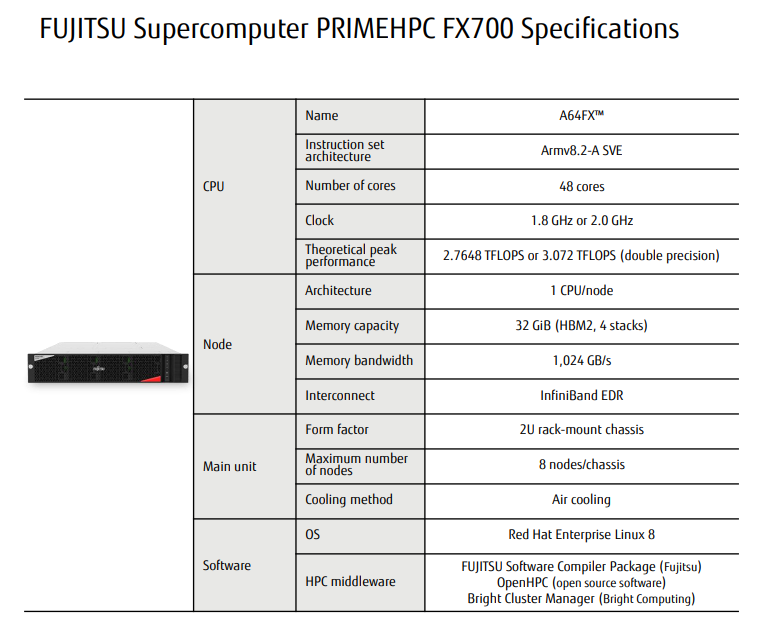
It wasn’t ever clear if the A64FX module would be available on a wider scale beyond supercomputer sales, however today confirms that it is, with the Japanese based HPC Systems set to offer a Fujitsu PrimeHPC FX700 server that contains up to eight A64FX nodes (at 1.8 GHz) within a 2U form factor. Each note is paired with 512 GB of SSD storage and gigabit Ethernet capabilities, with room for expansion (Infiniband EDR etc). The current deal at HPC Systems is for a 2-node implementation, at a price of ¥4,155,330 (~$39000 USD), with the deal running to the end of the year.

The A64FX card already has listed support for quantum chemical calculation software Gaussian16, molecular dynamics software AMBER, non-linear structure analysis software LS-DYNA. Other commercial packages in the structure and fluid analysis fields will be coming on board in due course. There is also Fujitsu’s Software Compiler Package v1.0 to enable developers to build their own software.
Source: HPC Systems, PDF Flyer
Related Reading
- New #1 Supercomputer: Fugaku in Japan, with A64FX, take Arm to the Top with 415 PetaFLOPs
- A Success on Arm for HPC: We Found a Fujitsu A64FX Wafer
- Hot Chips 2018: Fujitsu's A64FX Arm Core Live Blog


32 Comments
View All Comments
Oxford Guy - Saturday, June 27, 2020 - link
The creativity of these people is off the charts.sing_electric - Monday, June 29, 2020 - link
That was my first thought when I saw Fujitsu's choice of name for the processor. I'm not sure what marketing agency they use, but I'll bet they also pitched using the name 'Camry' to Honda or something.Sahrin - Friday, June 26, 2020 - link
This architecture kind of begs the question, what does an x86 CPU with HBM on-package perform like? There aren't a massive number of bandwidth-constrained applications, but those that are also tend to be ones where the x86 FPU (which is a monster as currently constituted) would enjoy the bandwidth.jeremyshaw - Friday, June 26, 2020 - link
CPUs do have a tendency of making up for this shortfall by using a lot of cache. 256MB of L3 on the best x86 setups, Power9 goes even wilder with complicated cache and memory system setups (which are claiming 350GB/s for their memory system). Even something like the massive GA100 only has 40MB of last level cache available.That being said, latest Intel setup is ~140GB/s (2933, 6 channel), latest AMD is ~200GB/s (3200, 8 channel). Sure, GDDR6 can go higher (at the cost of latency) and HBM can go even faster but I think part of a CPU's FPU performance is deep integration into the execution pipeline, using the same registers and cache hierarchy. Memory bandwidth alone would not be the main performance differentiator.
However, I would also like to see a HBM2 high performance x86 CPU, or at least good reasons why they don't exist.
Kevin G - Friday, June 26, 2020 - link
The biggest benefit for HBM isn't necessarily bandwidth but a potential reduction in memory latency. The amount of time to access HBM is lower than commodity DRAM.There is operational parallelism with HBM too as each 1024 bit wide stack necessitates is own independent memory controller: performing three reads and one write operation across four stacks is not an issue. Desktop systems generally have a single memory controller and Xeon's tend to have two with AMD's Epyc matching the figure at four. Future generations of HBM have the possibility of incorporating independent read/write buses plus seperate address and command buses. While that would radically increase in the number of vias through an interposer, such changes would eliminate the need for turn-around times that DRAM has to account for.
HBM has enough capacity now for commodity PC work but the reason we don't see them (yet?) for general usage is simply down to cost. There is still a huge premium attached to HBM that doesn't make it viable in the razor thin margin of PCs. Servers could easily absorb the cost of HBM enabled chips but server workloads tend to leverage far more memory than can be put into a package with a CPU. Like you though, I'd love to see such a system.
saratoga4 - Friday, June 26, 2020 - link
>There is operational parallelism with HBM too as each 1024 bit wide stack necessitates is own independent memory controller: performing three reads and one write operation across four stacks is not an issue.HBM channels are 128 bits wide, so each 1024 bit stack has 8 fully independent channels. 4 stacks gives a total of 32 independent memory accesses concurrently.
schujj07 - Saturday, June 27, 2020 - link
Using HBM as a high speed L4 would for sure help performance for servers. The reason server CPUs have so much cache is because they can use it and it helps performance. In a virtualized environment you might have 30 VMs running on a single host. A good number of those VMs might only have 4-8GB RAM and be sitting idle most times. You have 8+GB L4 HBM at 1TB/sec and you could probably substantial increase performance.brucethemoose - Friday, June 26, 2020 - link
"good reasons why they don't exist."Price, price, and price.
According to this: https://semiengineering.com/whats-next-for-high-ba...
HMB2 is about $120/16GB stack, and that may not include the interposer and the extra testing/validation.
Oxford Guy - Saturday, June 27, 2020 - link
Plenty of enthusiasts would be willing to pay that.That's peanuts when compared with the Nvidia GPU tax.
brucethemoose - Monday, June 29, 2020 - link
Maybe, but every addition to the BoM is multiplied, and comes at the cost of other features (like, say, a bigger die).