TSMC Boosts CapEx by $1 Billion, Expects N5 Node to Be Major Success
by Anton Shilov on January 22, 2020 11:15 AM EST
TSMC is on track to begin high-volume production of chips using its 5 nm technology in the coming months, the company said in its conference call last week. While so far the number of 5 nm tape-outs is lower when compared to the number of 7 nm tape-outs several months before production start, TSMC expects the process to become a major commercial success. Meanwhile, to ensure that it has no production constraints, the company plans to increase its 2020 CapEx by $1 billion.
It is well known that TSMC’s N5 manufacturing technology provides substantial improvements over the company’s N7 fabrication process (1.8x higher transistor density, +15% frequency or -20% power consumption), so major customers of the company are more than inclined to adopt it. TSMC is on track to start high volume manufacturing (HVM) using the technology in the first half of this year. So far, the number of N5 tape-outs is lower when compared to the number of N7 tape-outs at the same stage of development (i.e., several months before HVM) becase alpha customers have taped out a slightly lower number of N5 designs and other clients are yet to catch up. Meanwhile, TSMC remains optimistic about the technology’s ramp and expects N5 revenue to account for 10% of its 2020 wafer sales revenue, which essentially means that business performance of N5 in its first year will be the same as business performance of N7 in its first year.
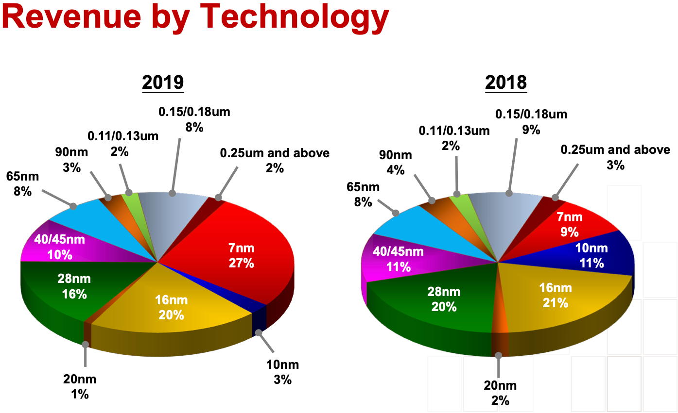
There are several reasons why TSMC’s N7 node turned out to be a huge commercial success for the foundry. First up, most of its customers skipped the 10 nm node and were more than motivated to go with 7 nm. Secondly, TSMC did not have a strong competition with its N7 technology: GlobalFoundries pulled out of the 7 nm race, whereas Samsung Foundry hardly processed any significant number of wafers using its 7LPP process. Thirdly, because N7 is a considerably more complex technology than TSMC’s 16 nm or 10 nm nodes, the company charges more money per wafer than before, which drives a greater revenue share for the process.
C. C. Wei, Vice Chairman and CEO of TSMC said the following:
“The 5 nm tape-out is little bit less than 7 nm compared at the same stage of the time. However, the most important thing is that the high-volume tape-out is almost equal. So, we expect that our 5 nm ramp is a very fast and smooth and it will contribute about 10% to this year's revenue."
Since TSMC’s N7 is considered as a long-living node, demand for the process is not expected to drop radically when N5 enters HVM, as there are tens of fabless semiconductor developers waiting to produce their 7 nm designs. Apparently, to satisfy demand for chips made using TSMC’s N7, N7+, N7P, N6, N5, and N5P manufacturing technologies (and offer some additional capacity for specialty processes as well as for advanced packaging), the company will have to further increase its 2020 CapEx by a billion of dollars up from $14 billion - $15 billion estimated last year.
TSMC does not say exactly how the additional $1 billion will be spent, but since in the coming quarters it will be ramping production using four process technologies that that use extreme ultraviolet lithography (EUVL) for select layers (up to 14 layers in case of N5, up from 4 and 5 in case of N7+ and N6) and multipatterning for some others, it is likely that the foundry is going to need some additional leading-edge equipment.
Wendell Huang, VP and CFO of TSMC, said the following:
“Other than the advanced technology, we also mentioned earlier, we also increased the CapEx this year for specialty technology as well as advanced packaging. So those are the areas that we are focusing on.”
Related Reading:
- TSMC: 5nm on Track for Q2 2020 HVM, Will Ramp Faster Than 7nm
- TSMC Radically Boosts CapEx to Expand Production Capacities, To Reach $14B For 2019
- Early TSMC 5nm Test Chip Yields 80%, HVM Coming in H1 2020
- TSMC: N7+ EUV Process Technology in High Volume, 6nm (N6) Coming Soon
Source: TSMC


40 Comments
View All Comments
Amandtec - Thursday, January 23, 2020 - link
Those kind of comments made sense years ago. Now the real test is how well the node performs in benchmarks and how much it costs e.g. Intel (presumably) never used 10nm for desktop because it's performance/yield was worse than 16nm++++.FreckledTrout - Thursday, January 23, 2020 - link
There is no standard measurement. Mostly because the transistors went 3D with FinFET and the nm size stopped mattering at that point. Really we as techies should give our own ratings to these based of densities. TSMC's 7nm node only has a very few up front features at 7nm the rest of the chip has larger features which is why Intel's 10nm is more like TSMC 7nm.yeeeeman - Friday, January 24, 2020 - link
It is marketing not real physical sizes they talk about.levizx - Saturday, January 25, 2020 - link
So you'll also find it interesting Cortex A76@3GHz is around Intel@1GHz?Santoval - Wednesday, January 22, 2020 - link
I would easily bet half of my money in the bank that Intel are not going to release any 7nm part in 2021, not even a "let's pull the wool over the eyes of our investors" semi-disabled 2-core i3 part, like they did with Cannon Lake. I rather predict a low volume 7nm "launch" (i.e. a little more than a paper launch) in 2022 and a high volume (the one that only matters) release in 2023. By that time TSMC will be at 3nm and GAA, and Samsung should not be far behind.If Intel do not pull an early 2021 high volume release of 7nm parts they will lose the next round of "process node wars" as well. And there's no way in hell they're going to achieve that feat.
Hulk - Wednesday, January 22, 2020 - link
Actually I think that's a good prediction based on past history.FreckledTrout - Thursday, January 23, 2020 - link
Not really. How many times has Intel goofed two generations? Never. Its his money but I wouldn't bet against Intel faltering two times in a row.Korguz - Thursday, January 23, 2020 - link
maybe.. but seems intels words.. are worth nothing now.. most are " ill believe it when it happens " view with intel now...yeeeeman - Friday, January 24, 2020 - link
That is because you don't have a clue how manufacturing works and how big of a problem you have when you test a process that doesn't work as you expect.There are two aspects:
1. marketing guys are trying to sugar coat the problem as much as possible. They get feedback from fab guys that they try something that might work. They translate it as the process will be up and running in one year. So on and so forth.
2. Fab engineers that - if asked - but no one will let them talk to the general public will say that maybe they don't know yet why it doesn't work or they understand why it doesn't, but they are trying to find a fix. Probably at some point they said, screw it, lets start from scratch with 10nm and build it on the base of 14nm. That is what we have today and this takes a LOT of time to get up and running.
So yeah, if you wanna believe the marketing guys talking about tech stuff, do it as you want. But I can tell you that when a process starts to work and the yields stabilize that means the dudes at the fab are starting to get the grasp of things and will work their way from there. And it seems like 10nm stuff is now stable. Ice Lake products are plentiful, prices are decent so I don't see any reason they won't continue executing well with 7nm. From their earnings call, they should have a GPU at 7nm (ponte vechio) in 2021 and a CPU in 2022. Which does fit with TSMC 5nm process.
Korguz - Friday, January 24, 2020 - link
and most of the public also doesnt understand it too.. go accuse them as well.... whats your point ?? most of the public.. seems to be tired of intels lies and its " sugar coating " as you put it.. IF intel had been open and honest about how much they screwed up worh 10nm.. and admit they were too aggressive with it.. then maybe there would be a bit more understanding.. but nope.. they kept lieing about it.. kept saying its on track.. and it still is broken...