Qualcomm Announces Snapdragon 675 - 11nm Mid-Range Cortex A76-Based
by Andrei Frumusanu on October 22, 2018 9:00 PM EST- Posted in
- Smartphones
- Qualcomm
- Mobile
- SoCs
- 11LPP
- Snapdragon 675
Today we’re seeing a very interesting announcement from Qualcomm: The new Snapdragon 675 chipset is a direct successor to the current generation Snapdragon 670 which was only announced back in August. The Snapdragon 675 iterates on the current design, bringing some important upgrades.
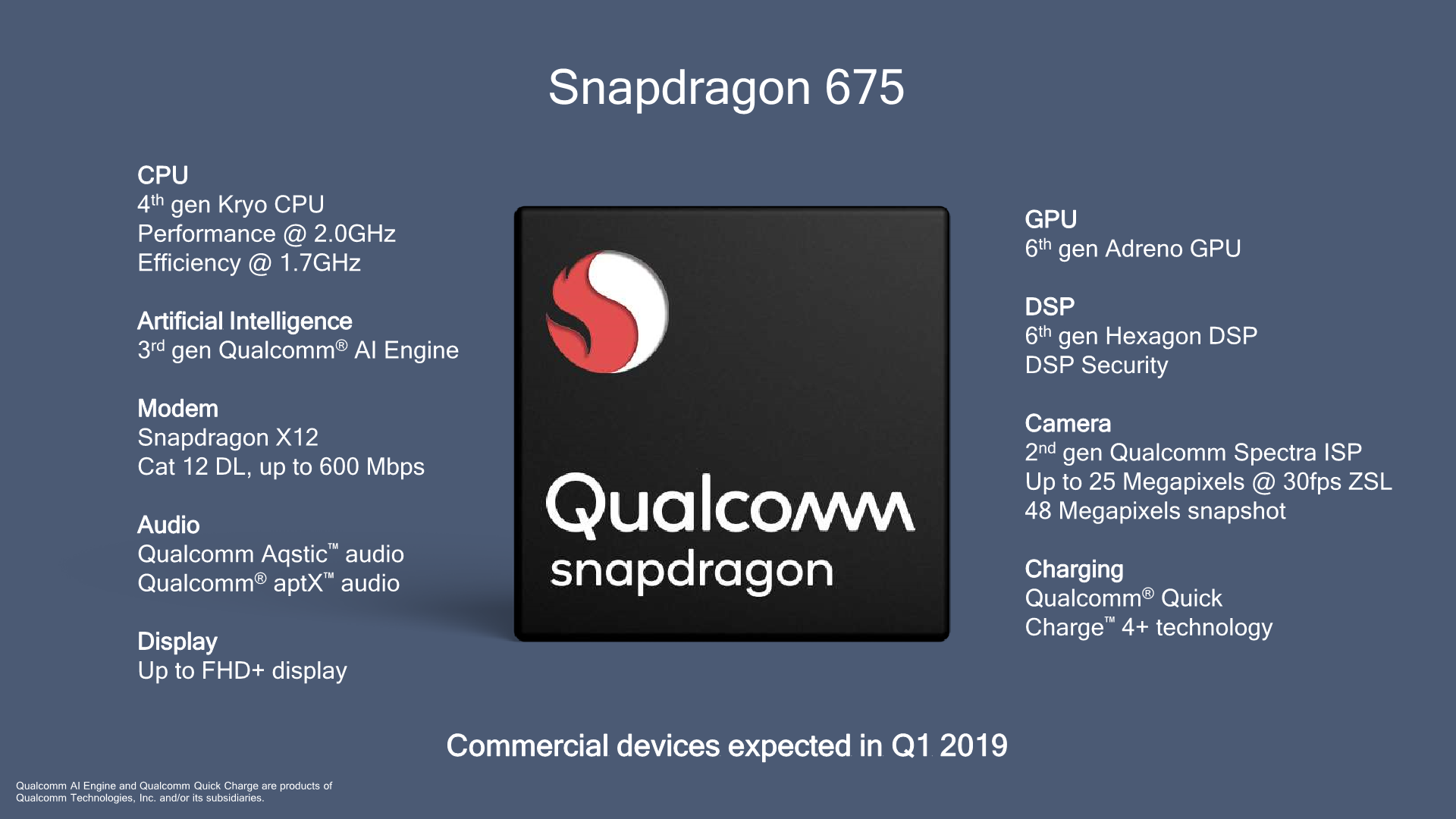
| Qualcomm Snapdragon Upper Mid-Range SoCs | |||
| SoC | Snapdragon 670 | Snapdragon 710 | Snapdragon 675 |
| CPU | 2x Kryo 360 (CA75) @ 2.0GHz 6x Kryo 360 (CA55) @ 1.7GHz |
2x Kryo 360 (CA75) @ 2.2GHz 6x Kryo 360 (CA55) @ 1.7GHz |
2x Kryo 460 (CA76) @ 2.0GHz 256KB L2 6x Kryo 460 (CA55) @ 1.7GHz 64KB L2 |
| GPU | Adreno 615 | Adreno 616 | Adreno 612 |
| DSP | Hexagon 685 | ||
| ISP/ Camera |
Spectra 250 ISP 25MP single / 16MP dual |
Spectra 250 ISP 32MP single / 20MP dual |
Spectra 250 ISP triple-camera support |
| Memory | 2x 16-bit @ 1866MHz LPDDR4X 14.9GB/s 1MB system cache |
||
| Integrated Modem | Snapdragon X12 LTE (Category 15/13) DL = 600Mbps 3x20MHz CA, 256-QAM UL = 150Mbps 2x20MHz CA, 64-QAM |
Snapdragon X15 LTE (Category 15/13) DL = 800Mbps 3x20MHz CA, 256-QAM UL = 150Mbps 2x20MHz CA, 64-QAM |
Snapdragon X12 LTE (Category 12/13) DL = 600Mbps 3x20MHz CA, 256-QAM UL = 150Mbps 2x20MHz CA, 64-QAM |
| Encode/ Decode |
2160p30, 1080p120 H.264 & H.265 |
2160p30, 1080p120 H.264 & H.265 |
2160p30, 1080p120 H.264 & H.265 |
| Mfc. Process | 10nm LPP | 11nm LPP | |
The new SoC platform is Qualcomm’s first to employ the newest generation “Kryo 460” CPU microarchitecture. Obviously Qualcomm is still using Arm’s “Built on Arm Cortex Technology” CPU license, meaning the SoC uses a customised order of the Arm IP. What is very exciting to see is that the Snapdragon 675’s Kryo 460 performance CPUs are based on the new Cortex A76 cores. I think this is the first time that a SoC vendor actually introduces a new CPU microarchitecture in a mid-range product first, as I had expected Qualcomm to unveil it in the upcoming Snapdragon flagship.
The performance cores come in a 2x configuration clocking at up to 2GHz, accompanied by 6x Cortex A55 derived efficiency cores, running at up to 1.8GHz.
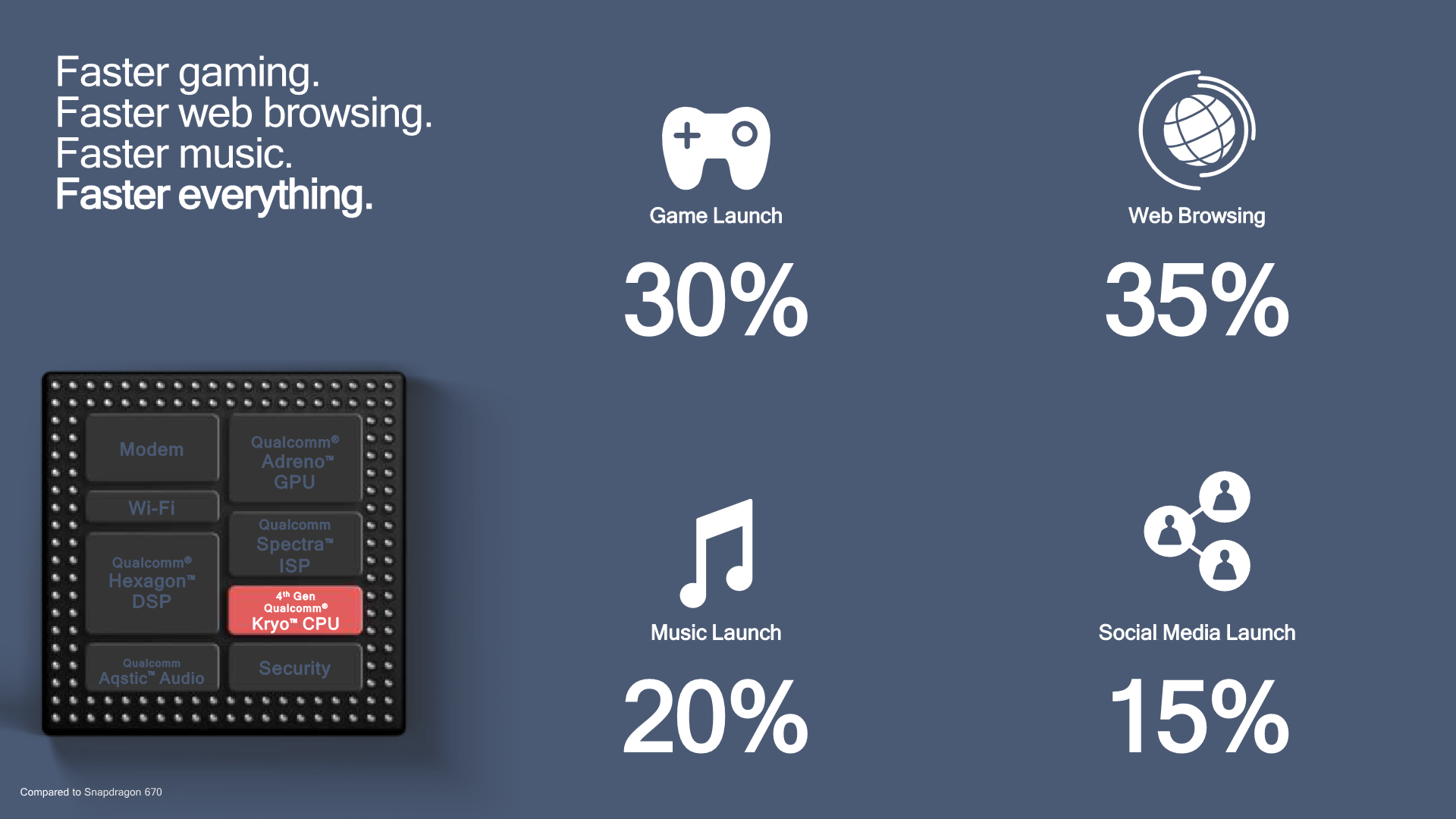
The CPU performance improvements over the Snapdragon 670’s Cortex A75-based Kryo setup are quoted by Qualcomm to range from 15% in app launches, up to 35% in web browsing scenarios. This roughly matches Arm’s claims of the IPC improvements of the new microarchitecture, and because the Snapdragon 675 is running at the same clock as the Snapdragon 670, the performance improvements are actually due to just the new generation cores.
What also is quite weird is that the new SoC should in effect also outperform the Snapdragon 710 – even though the latter is in a higher tier segment. We’ll likely see a successor to this platform sometime in the future.
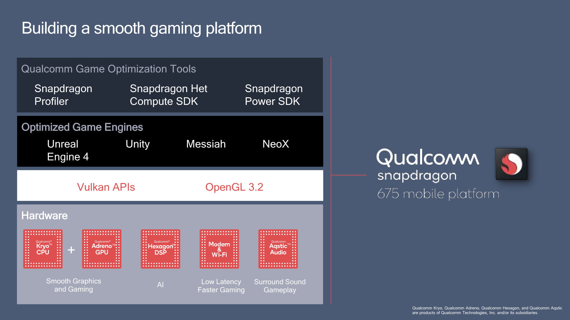
As of time of writing, Qualcomm didn’t talk much about raw performance improvements of the GPU. It’s still an Adreno 61x series GPU, and I expect it to be in the performance range of the Adreno 615 or 616.
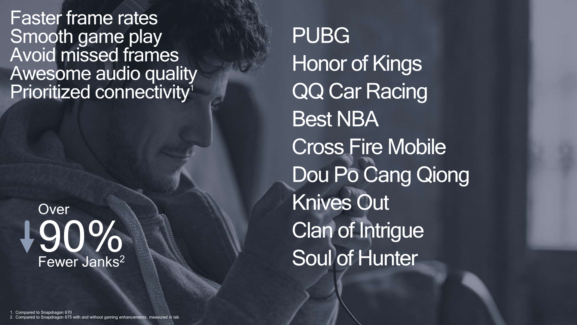
What Qualcomm did talk about, is that the new SoC employs some sort of software “gaming enhancements” that promise up to 90% fewer janks. Again I followed up with a request with more technical explanation as to what this is, but with no official response as of yet. What is very obvious here is that this sounds strikingly similar to Huawei/Honor’s “GPU Turbo” mechanism in what it promises to achieve. Hopefully we’ll have a more detailed explanation in the future. Similar to GPU Turbo, these gaming enhancements appear to be game title specific.

An improvement on the ISP side is the new support for seamless triple-camera setups. The new Snapdragon 675 adds an additional MIPI CSI port, totalling up to three. This allows the new SoC to be able to operate three cameras at once, which is something that will seemingly become very popular in the comings months as more devices with telephoto, wide-angle, and super-wide angle modules are announced. Here the ISP hardware needs to be capable of enough in terms of throughput to deal with the large amount of pixel data from the sensors.

Qualcomm enables the hardware and software to support both bokeh (portrait modes) and HDR shots in a single shot. Bokeh effects are supported by multiple techniques; either stereo depth sensing via dual cameras, active depth sensing via time-of-flight, or just simply by a single camera sensor which has phase detection pixels.
First Samsung 11nm “11LPP” product?
What surprised me even more than the announcement of a Cortex A76 mid-range SoC, was the revelation that it’s manufactured on Samsung’s new 11LPP manufacturing node. Samsung’s 11nm node is a mix of its 14 and 10nm nodes, and is targeted for cost-effective solutions while still maintaining performance competitiveness with the 10nm products.
Qualcomm didn’t talk much about power efficiency of the Snapdragon 675, and it’s likely that we won’t be seeing any major improvements.
Again it’s remarkable to see Qualcomm having such short product refresh cycles in this range, as seemingly competition is fierce and pricing in the mid-range is a cut-throat business in order to achieve design wins.
The big remaining question is where and when does the Snapdragon 675 position itself against its current counter-parts? The new SoC is scheduled to be available in commercial devices in Q1 of 2019. As Snapdragon 670 devices have already started to launch, the two products will co-exist with each other for some time.
Related Reading
- Qualcomm Reveals The Snapdragon 670 Platform: Dual Big Cores + Adreno 615
- Samsung Details 11LPP Process Technology: 10 nm BEOL Meets 14 nm Elements
- Qualcomm Announces Snapdragon 710 Platform
- Qualcomm Announces Snapdragon 700 Series Platform: Carving Out A Niche for Sub-Premium
- The Snapdragon 845 Performance Preview: Setting the Stage for Flagship Android 2018
- Qualcomm Announces Snapdragon 660 & 630 Mobile Platforms: Better Connectivity, Camera, & Compute at 14nm


40 Comments
View All Comments
djayjp - Monday, October 22, 2018 - link
Maybe Janks are a good thing... maybe we want MORE Janks!?!PeachNCream - Tuesday, October 23, 2018 - link
Really though, what is are Janks? Is that like application hesitation or a period of reduced framerate? Even the tiny text at the bottom of the slide doesn't define it and I've never heard the term before. It sounds like a made up work.Ryan Smith - Tuesday, October 23, 2018 - link
"Janky" is typically used to describe sudden leaps in frametimes. Say a frame taking 100ms instead of 16ms.serendip - Monday, October 22, 2018 - link
Qualcomm and their ultra-confusing lineup... The 636, 660 and 710 are closely related but the 636 and 660 are getting more design wins. The 710 is probably priced too high and too close to the 845 in terms of performance.I've used Mi 8's with the 660 and 710 chips, I can't tell any difference between them in normal use and the 660 is more than good enough. My old 650 still rocks against a lot of newer chips although power consumption is higher.
tinted - Tuesday, October 23, 2018 - link
For me new chips makes sense because of the new ISP and other things that gets upgraded along with the efficiencyPerformance is also good to have but for my usage that does not make any difference
Dragonstongue - Tuesday, October 23, 2018 - link
those configs are WEIRD ASF.most of this I understand (kind of) but 6 cores at higher clock to chew battery even more and 11nm..totally weird.
Likely because it is Samsung and "claimed" higher performance it will also have a higher price because of such (real world "gain" likely to be at the very most in the range of tops ~2% mixed usage performance at probably an extra 5% battery use) because having a good size battery in these super easy to shatter phones is impossible, but yet they figure out how to make them thinner and thinner.
>:(
so they increase clock rate for the 6 core (600Mhz combined) reduced clock on the 2 core (400mhz combined) reduction in the modem capability by 200Mhz as well....hmmm, it is QC after all, but I do not picture this being "faster" at all, (marketing is very rarely real world accurate)
though some of the 7nm stuff looks VERY promising.
Unless they dropped volts or something that much more on the 6 cores and lost a bit of speed modem wise which helped it "sip power" even more and did some extra fancy trickery to make sure use least amount of power possible while always in maximal performance mode something along those lines.
but seriously 11nm da fook..bad enough everyone is playing with die shrink naming these days, now they are "mix and matching" to confused naming even more...I guess when folks see 10nm it might back fire in their face because "oh this must be older gen, I think I will go to the "smaller" number instead"
Or they are just trying to get each other all "wound up" with their fancy moronic naming game??
They might as well just start calling them by the chip model number and nothing more, it is getting out of hand.
on another note, if they can do really silly chip designs i.e BIG.little that have very little difference in clock speed seemingly to "hurt" performance more then "help" battery life, why not just go way out there and do 2 cores at a high speed, 2 or 4 cores at medium and 2 at low speed so they could ensure highest possible performance at lowest power usage no matter what the device is doing, hell it might "allow" the 2 slowest cores worry about all the background crd so the higher performing cores can worry about the "heavy lifting" or something.
Let us call it BIG.Little.micro design ^.^
Wilco1 - Tuesday, October 23, 2018 - link
Man you've got issues...The first thing you need to try to understand that not all cores are equal. A newer more advanced core will outperform an older core even when running at a significantly lower frequency. So yes, this is definitely much faster than the 710. Also a big core could run at 800MHz and still be faster than a little core at 1.7GHz. And maximum clock frequency as listed is just that. If there is not much work to do the active cores will run at a much lower frequency (to gain power efficiency) and some cores will be switched off.
haukionkannel - Tuesday, October 23, 2018 - link
Most likely 11nm is 14++ version with marketing coating... based on the 14 nm variant info from article.Shekels - Tuesday, October 23, 2018 - link
What the hell have you been smoking... 11nm is the physical size of the transistor. 14++ is still a 14nm transistor. 11nm is much closer to 10nm than 14nm... There is no way the 11nm is 14++ but marketed differently. That would be false informationWilco1 - Tuesday, October 23, 2018 - link
11nm is an improved 14nm process with 10% higher density and 15% better performance. See the link at the bottom of the article: https://www.anandtech.com/show/11877/samsung-detai...Note the nm figure hasn't referred to physical transistor size for more than 10 years now.