Samsung Starts Production of 8 Gb DDR4-3600 ICs Using 2nd Gen 10nm-Class Tech
by Anton Shilov on December 20, 2017 10:00 AM EST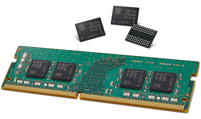
Samsung late on Wednesday said that it had initiated mass production of DDR4 memory chips using its second generation '10 nm-class' fabrication process. The new manufacturing technology shrinks die size of the new DRAM chips and improves their performance as well as energy efficiency. To do that, the process uses new circuit designs featuring air spacers (for the first time in DRAM industry). The new DRAM ICs (integrated circuits) can operate at 3600 Mbit/s per pin data rate (DDR4-3600) at standard DDR4 voltages and have been validated with major CPU manufacturers already.
As it usually happens with Samsung’s major DRAM-related announcements, the news today consists of two parts: the first one is about the new DDR4 IC itself, the second part is about the second generation '10 nm-class' (which Samsung calls '1y' nm) manufacturing technology that will be used for other DRAM products by the company. Both parts are important, but let’s start with the new chip.
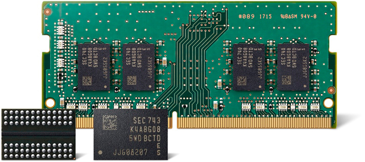
Samsung’s new DDR4 chip produced using the company’s 1y nm fabrication process has an 8-gigabit capacity and supports 3600 MT/s data transfer rate at 1.2 V. The new D-die DRAM runs 12.5% faster than its direct predecessor (known as Samsung C-die, rated for 3200 MT/s) and is claimed to be up to 15% more energy efficient as well. In addition, the latest 8Gb DDR4 ICs use a new in-cell data sensing system that offers a more accurate determination of the data stored in each cell and which helps to increase the level of integration (i.e., make cells smaller) and therefore shrink die size.
Samsung says that the new 8Gb DDR4 chips feature an “approximate 30% productivity gain" when compared to similar chips made using the 1x nm manufacturing tech. UPDATE 12/21: Samsung clarified that productivity gain means increase in the number of chips per wafer. Since capacity of Samsung's C-die and D-die is the same, the increase in the number of dies equals the increase in the number of bits per wafer. Therefore, the key takeaway from the announcement is that the 1y nm technology and the new in-cell data sensing system enable Samsung to shrink die size and fit more DRAM dies on a single 300-mm wafer. Meanwhile, the overall 30% productivity gain results in lower per-die costs at the same yield and cycle time (this does not mean that the IC costs are 30% lower though) and increases DRAM bit output.
Samsung does not release exact smallest hhalf-pitchsize of the new DRAMs (the feature size used to give names to DRAM process technologies), so at this point we do not know any details about the new chip’s geometries. Given that we are dealing with a 1y process, it logical to assume that the smallest half pitch size is from 14nm to 16 nm, but this is a speculation at this point. What we do know is that Samsung’s 1y nm process technology continues to use ArF (argon fluoride) immersion lithography tools presumably with quadruple patterning (so no EUV). Meanwhile, to reduce parasitic capacitance, Samsung placed air spacer around its bit lines, which helps to increase DRAM performance.
Speaking of performance, it is noteworthy that Samsung’s C-die DRAMs have not been used by companies like Corsair and G.Skill for their leading-edge memory modules for enthusiasts. Apparently, both companies still use the time-proven Samsung B-die ICs made using 20 nm process technology. It remains to be seen whether the aforementioned manufacturers jump to the new 1y nm 8 Gb DDR4 ICs and when.
Samsung says that the new in-cell data sensing system as well as air spacers will be used to make other types of DRAM, including DDR5, HBM3, LPDDR5, and GDDR6 — meaning that these two elements will be used for years to come. Of course, it will be a while before the first three standards enter commercial production, but GDDR6 with the aforementioned enhancements could be produced in the foreseeable future and using the 1y nm process.
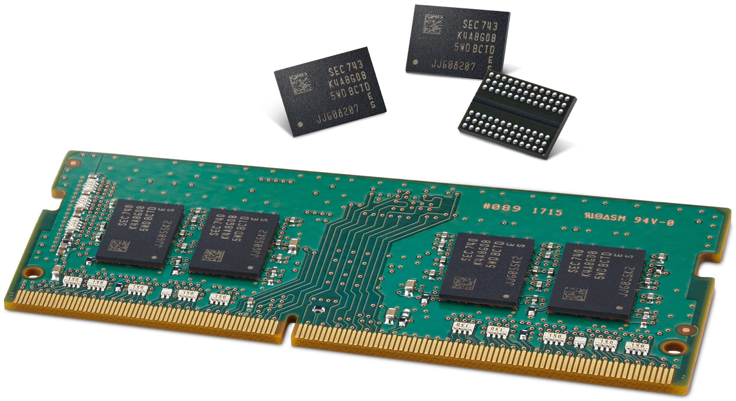
CPU developers (likely Intel, AMD, IBM, Qualcomm, etc.) have already validated the new 8 Gb DDR4-3600 memory chips produced using Samsung’s 2nd generation 10 nm-class process technology. The next step for Samsung is to validate memory modules with PC makers and put these modules into the next-gen systems. It is noteworthy that this time Samsung only displays the new 8 Gb ICs on an SO-DIMM, but not on a desktop-class memory module. It is unknown whether this has something to do with product positioning and/or Samsung's own plans for modules (e.g., laptops are addressed first), but previously Samsung always published pictures of its latest DRAMs both on DIMMs and SO-DIMMs.
Along with the announcement of the new 8 Gb DDR4 DRAM IC, Samsung also said that it would ramp up production of memory (not only DDR4, but also mobile DRAM, etc.) using both of its 10 nm-class fabrication processes to meet “growing demand for DRAM in premium electronic systems worldwide”.
Related Reading
- Samsung Begins To Produce DDR4 Memory Using '10nm Class' Process Tech
- Samsung Pre-Announces 16 Gbps GDDR6 Chips for Next-Gen Graphics Cards
- Samsung Starts Production of 512 GB UFS NAND Flash Memory: 64-Layer V-NAND, 860 MB/s Reads
- Samsung Starts Mass Production of Chips Using 10nm Low Power Plus (10LPP) Process Tech
- Samsung’s 8LPP Process Technology Qualified, Ready for Production
- Samsung Details 11LPP Process Technology: 10 nm BEOL Meets 14 nm Elements
Source: Samsung


24 Comments
View All Comments
MrSpadge - Wednesday, December 20, 2017 - link
DDR4-3600 at stock voltage - impressive! Now JEDEC and Ryzen's memory controller should better catch up a bit.CheapSushi - Thursday, December 21, 2017 - link
I really hope Zen+ or Zen2 use higher speeds for ECC; current 2400MHz is just a bit cripple for AMD EPYC. Current certified JEDEC ECC standard is 3200MHz, yet no kit exists in the wild and no system supports it. These 3600 ICs sound amazing. I hope we get to use them.Snowleopard3000 - Sunday, December 31, 2017 - link
So does this mean that high end laptops like Sager, MSI, Eurocom, Origin with 4 x ram slots will now support 128gb of DDR-4 ram or are they still limited to 64gb of DDR-4 ram?RavenRampkin - Tuesday, August 4, 2020 - link
The year is 2020, these are unicorns.