GlobalFoundries Weds FinFET and SOI in 14HP Process Tech for IBM z14 CPUs
by Anton Shilov on September 22, 2017 7:00 AM EST- Posted in
- CPUs
- GlobalFoundries
- IBM
- Semiconductors
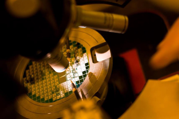
GlobalFoundries this week formally introduced its new custom process technology that will be used to manufacture IBM's z14 CPUs, which in turn were announced earlier this year. The 14HP (14 nm, high performance) tech weds FinFET transistors and SOI substrates to get IBM the best of both worlds: small feature sizes and maximized clockspeed potential.
When IBM and GlobalFoundries agreed to transfer semiconductor manufacturing business of the former to the latter, IBM demanded GF to develop and offer custom fabrication processes for IBM’s server CPUs throughout 2014 to 2024 timeframe and involving multiple nodes. Initially the companies talked about custom 22 nm, 14 nm and 10 nm technologies, but in their final announcement they only mentioned a 10-year exclusive supply agreement without disclosing particular nodes. Therefore, it remains to be seen what GlobalFoundries, which is skipping the 10 nm node, is going to offer to its partner (a custom 7 nm is a natural guess). Earlier this year IBM announced its z14 processors for mainframes and this week GlobalFoundries disclosed details about the process technology used to make these chips.
Before we proceed to 14HP, let’s recap what is the IBM z14 and why the blue giant needed a custom technology to build it. The IBM Z mainframes are designed for 24/7/365 availability with zero downtime and are aimed at mission critical applications like credit card processing. IBM Z mainframes are based on specially designed IBM z-series CPUs, which are unique both in terms of microarchitecture, feature set and even physical layout. Each IBM Z14 blade features six CPUs (which IBM calls CPs) carrying processing cores and L2+L3 caches as well as a system control chip (which IBM calls SC) featuring a large L4 cache as well as various interconnects. Each IBM z14 SC CPU consists of 6.1 billion transistors, runs at 5.2 GHz and contains 10 cores with dedicated 6 MB L2 per core (2MB L2 for instructions, 4MB L2 for data) and 128 MB shared L3. Meanwhile, the system control (SC) chip consists of 9.7 billion transistors and features 672 MB of L4 and interconnects to ensure coherency between CPUs. Needless to say, that both CP and SC are extremely complex and benefit from manufacturing technologies with small feature sizes.
Being very complex and very fast, IBM’s CPUs for z-series mainframes were historically produced using custom fabrication processes that were architected to deliver maximum performance, manufacturing costs be damned. In fact, it was IBM whom first used SOI substrates to build its RS64-IV codenamed ‘Istar’ PowerPC-AS CPUs in 2000, which was then followed by AMD and others whom used SOI to build their own highly-successful processors. The use of SOI enables a tangible increase of CPU clock rates without a massive increase of power consumption, but a SOI wafer substrate costs more than a bulk substrate, so this is exactly what GlobalFoundries’14HP is about.
| Comparison of 14 nm Branded Process Technologies | |||||||
| GlobalFoundries 12LP |
GlobalFoundries 14HP |
GlobalFoundries 14LPP ? |
TSMC 16FF |
Intel 14nm |
|||
| Fin Pitch | ? | ? | ? | ? | 42 nm | ||
| Gate Pitch | ? | ? | 78 nm | 90 nm | 70 nm | ||
| Min Metal Pitch | ? | ? | 64 nm | 64 nm | 52 nm | ||
| Gate Height | ? | ? | less than 480 nm | 480 nm | 399 nm | ||
| Metal Layers | 13 | 17 | 13 | unknown | unknown | ||
| Design Library | 7.5T | 12T | 9T | 9T | unknown | ||
GlobalFoundries says that the 14HP process technology leverages “the proven 14nm FinFET high-volume experience of our Fab 8 facility”, but does not explicitly say that 14HP is based on 14LPP; only that it uses SOI substrates instead of bulk ones. In fact, looking at the numbers it appears to be substantially different. When compared to GF’s 14LPP and similar bulk FinFET process technologies, 14HP can support up to 17 metal layers (vs. 13 for the 14LPP) and uses 12T libraries (vs. 9T and 7.5T for various 14 nodes). As for experience, 14HP will be utilized across the same ASML TWINSCAN NXT scanners that the company uses to produce existing chips using its current FinFET technologies.
GlobalFoundries is not disclosing too many specific details about 14HP, which isn't all that surprising given the situation at hand. There is a single customer that is going to use it, and IBM does not want to share too many details about how it designs its processors as well. So, while we do understand that SOI can help with increasing frequencies and voltages compared to bulk process technologies, we do not have precise numbers here.
Related Reading:
- Hot Chips: IBM's Next Generation z14 CPU Mainframe Live Blog (5pm PT, 12am UTC)
- GlobalFoundries and AMD Announce First 14nm FinFET Sample Production Success
- GlobalFoundries Adds 12LP Process for Mainstream and Automotive Chips; AMD Planning 12LP CPUs & GPUs
- GlobalFoundries Details 7 nm Plans: Three Generations, 700 mm², HVM in 2018
- GlobalFoundries to Expand Capacities, Build a Fab in China
- GlobalFoundries Updates Roadmap: 7 nm in 2H 2018, EUV Sooner Than Later?
Source: GlobalFoundries


31 Comments
View All Comments
Adele Hars - Sunday, October 1, 2017 - link
IBM's decision to go with FinFET on SOI dates back well over five years, and the physics have not changed in that time. If you're willing to take a bit of a deep dive, Terry Hook, who's IBM's SOI-FinFET holes & electrons guru, did a few pieces for Advanced Substrate News back in 2012/2013. I'll paste in links below.http://bit.ly/2xPCNIW - FinFET on SOI: Potential Becomes Reality
http://bit.ly/2yBtuKj - IBM: FinFET Isolation Considerations and Ramifications – Bulk vs. SOI
http://bit.ly/2kh4dTA - IBM: Why Fin-on-Oxide (FOx/SOI) Is Well-Positioned to Deliver Optimal FinFET Value
Also, the folks at the SOI Consortium laid it out in very simple terms (re: advantages of doing planar FD-SOI or FinFET-on-SOI) back in a 2012 piece -- you can find that here: http://bit.ly/2fCLTix.
And finally, a note for those worried about SOI wafer costs, the wafers are slightly more expensive, but that cost is immediately amortized because the manufacturing process in the fab uses fewer mask steps when the starting wafer is an SOI wafer. That holds for both FinFETs on SOI and FD-SOI, btw.