Intel Displays 10nm Wafer, Commits to 10nm ‘Falcon Mesa’ FPGAs
by Ian Cutress on September 19, 2017 8:30 AM EST
On the back of Intel’s Technology and Manufacturing Day in March, the company presented another iteration of the information at an equivalent event in Beijing this week. Most of the content was fairly similar to the previous TMD, with a few further insights into how some of the technology is progressing. High up on that list would be how Intel is coming along with its own 10nm process, as well as several plans regarding the 10nm product portfolio.
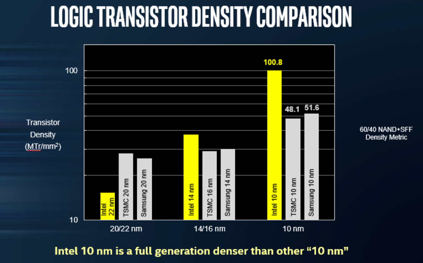
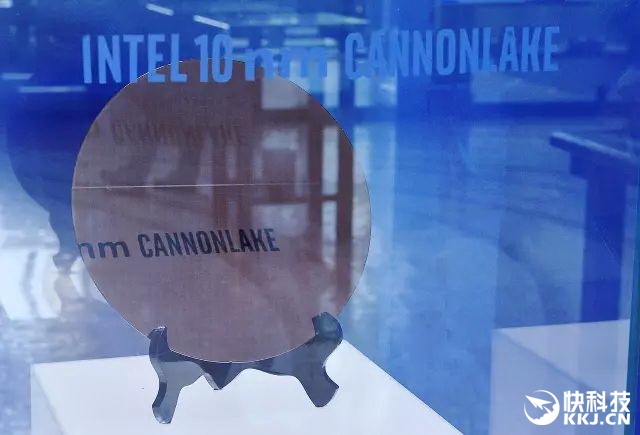
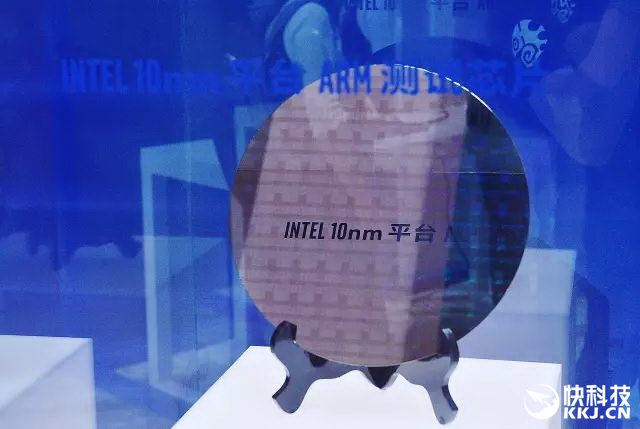
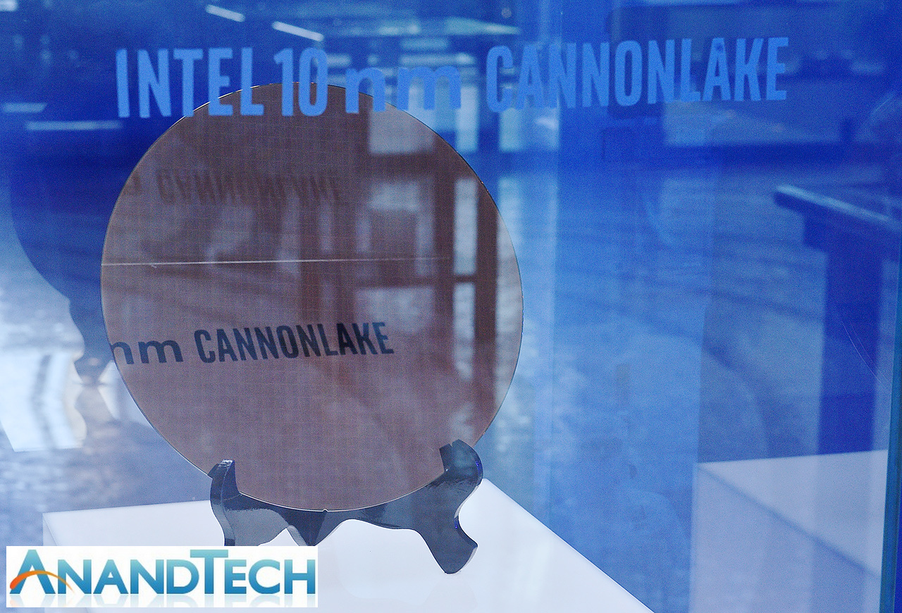
The headline here was ‘we have a wafer’, as shown in the image above. Intel disclosed that this wafer was from a production run of a 10nm test chip containing ARM Cortex A75 cores, implemented with ‘industry standard design flows’, and was built to target a performance level in excess of 3 GHz. Both TSMC and Samsung are shipping their versions of their ‘10nm’ processes, however Intel reiterated the claim that their technology uses tighter transistors and metal pitches for almost double the density of other competing 10nm technologies. While chips such as the Huawei Kirin 970 from TSMC’s 10nm are in the region of 55 million transistors per mm2, Intel is quoting over 100 million per mm2 with their 10nm (and using a new transistor counting methodology).
Intel quoted a 25% better performance and 45% lower power than 14nm, though failed to declare if that was 14nm, 14+, or 14++. Intel also stated that the optimized version of 10nm, 10++, will boost performance 15% or reduce power by 30% from 10nm. Intel’s Custom Foundry business, which will start on 10nm, is offering customers two design platforms on the new technology: 10GP (general purpose) and 10HPM (high performance mobile), with validated IP portfolios to include ARM libraries and POP kits and turnkey services. Intel has yet to announce a major partner in its custom foundry business, and other media outlets are reporting that some major partners that had signed up are now looking elsewhere.
Earlier this year Intel stated that its own first 10nm products would be aiming at the data center first (it has since been clarified that Intel was discussing 10nm++). At the time it was a little confusing, given Intel’s delayed cadence with typical data center products. However, since Intel acquired Altera, it seems appropriate that FPGAs would be the perfect fit here. Large-scale FPGAs, due to their regular repeating units, can take advantage of the smaller manufacturing process and still return reasonable yields by disabling individual gate arrays with defects and appropriate binning. Intel’s next generation of FPGAs will use 10nm, and they will go by the codename “Falcon Mesa”.
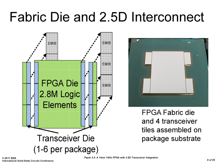
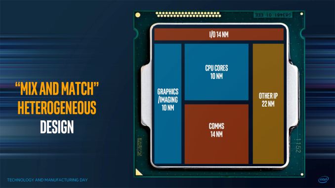
Falcon Mesa will encompass multiple technologies, most noticeably Intel’s second generation of their Embedded Multi-Die Interconnect Bridge (EMIB) packaging. This technology embeds the package with additional silicon substrates, providing a connection between separate active silicon parts much faster than standard packaging methods and much cheaper than using full-blown interposers. The result is a monolithic FPGA in the package, surrounded by memory or IP blocks, perhaps created at a different process node, but all using high-bandwidth EMIB for communication. On a similar theme, Falcon Mesa will also include support for next-generation HBM.
Possibilities with EMIB
Among the IP blocks that can be embedded via EMIB with the new FPGAs, Intel lists both 112 Gbps serial transceiver links as well as PCIe 4.0 x16 connectivity, with support for data rates up to 16 GT/s per lane for future data center connectivity. This was discussed at the recent Hot Chips conference, in a talk I’d like to get some time to expand in a written piece.
No additional information was released regarding 10nm products for consumer devices.
Related Reading
- Intel Officially Reveals Post-8th Gen Core Code Name: Ice Lake, Built on 10nm+
- Hot Chips: Intel EMIB and 14nm Stratix 10 FPGA Live Blog
- CES 2017: Intel Press Event Live Blog
- Samsung and TSMC Roadmaps: 8 and 6 nm Added, Looking at 22ULP and 12FFC


Additional: 1:00pm September 19th
After doing some digging, we have come across several shots of the wafer up close.
From http://news.mydrivers.com/
This is from the presentational display. Detail is very hard to make out at the highest resolution we can find this image.
Additional: 1:20pm September 19th
Intel has also now put the presentation up on the website, which gives us this close-up:

Surprisingly, this wafer looks completely bare. Either this is simply a 300mm wafer before production, or Intel have covered the wafer on purpose with a reflective material to stop prying eyes. It's a very odd series of events, as Intel did have other wafers at the event, including 10nm using ARM, and examples of the new 22FFL process.
From http://news.mydrivers.com/
 From http://news.mydrivers.com/
Both of these wafers seem to have a repeating pattern we would typically see on a manufactured wafer. So either Intel does not want anyone to look at 10nm Cannon Lake just yet, or they were just holding up an unused disc of silicon.
Additional: 3:00pm September 20th
Intel got back to us with a more detailed Cannon Lake image, clearly showing the separate dies:
Manual counting puts the wafer at around 36 dies across and 35 dies down, which leads to a die size of around 8.2 mm by 8.6 mm, or ~70.5 mm2 per die. At that size, it would suggest we are likely looking at a base dual-core die with graphics: Intel's first 14nm chips in a 2+2 configuration, Broadwell-U, were 82 mm2, so it is likely that we are seeing a 2+2 configuration as well. At that size, we're looking at around 850 dies per wafer.
Source: Intel


52 Comments
View All Comments
MrSpadge - Tuesday, September 19, 2017 - link
> So a metric that privileges memory density over logic density makes a company that ships with lots of logic on the chip look worse. Even if your metric includes both memory and logic transistors, who's to say what the appropriate weighting is?Apparently you completely misunderstood the point. This scheme is made to exactly combat what you're suggesting. It's calculating a density metric without taking the actual product produced on the process into account, as that's always going to vary in the fractions of memory, logic etc. Which is just what Intel is saying in the quote you're attacking later on.
There's really no point trying to compare PROCESSES when different chip designs are involved. That's what the competition did to Intel, and what they want to correct with this. This puts them in a better light, obviously, but not with an unfair advantage. So by "to give neither an advantage nor a disadvantage to anyone" I mean compared to how the different designs should technically be compared, not compared to what we previously had.
HStewart - Tuesday, September 19, 2017 - link
This sounds like to me a significant advancement in technology, but also explains why 10nm is taking so long to developed. Being able to pack twice ( possible 2 1/2 ) transistors in same space is really awesome. This could mean including twice as many cores in the same space.But Intel is extremely smart, they realize that such technology is expensive and for some components of the chip - like IO and communications, you don't need such technology.
I feel this is just a beginning and we are going see quite interesting in future. More transistors also means possibly that Intel will increase internal graphics levels.
name99 - Tuesday, September 19, 2017 - link
Seriously? The best they can show is a wafer?You don't think TSMC has 7nm wafers RIGHT NOW? The competition is not TMC 10nm today, it is whatever is around when Intel finally ships 10nm.
Right now it looks like Apple will be shipping the A11X on 7nm in April or May or so next year. Probably one of the top tier ARM vendors (QC? Huawei?) will also have one of their SoCs on TSMC 7nm at the same sort of time.
Meanwhile, let's look at Intel's record.
2011 announcement of Fab 42 to handle 14nm (which was then cancelled/postponed) [But don't worry, this time, for sure, Fab 42 is going to open one day, now equipped for 7nm ...]
Q3 2013 Intel demos a few 14nm Broadwells. Promises they'll be available Q4.
They were --- just Q4 2014...
Compare this round where we don't even have the demo chips working, just a wafer, and there isn't enough confidence to even suggest a shipping date.
This is not boasting from a position of strength. This is a desperate attempt to fool the rubes with a variety of smoke and mirrors (test wafers vs test chips vs shipping dates; comparing Intel in [two years?] with TSMC today rather than in two years; etc)
Notmyusualid - Tuesday, September 19, 2017 - link
Intel, typically tell the truth, regarding their lithography. If they say its 10nm, it is.I'm not sure what else you expect them to show you (and the competition)?
Maybe write them, ask for a tour of the 10nm fab, and let me know how you get on, and if you understood a dam thing.
Back in my Uni days, we used 'Chipwise', to design our own circuits. It was without doubt the most interesting part of my electronics degree.
Seeing some of the final-year projects blew me away. They had them blown-up to A1 posters on the wall. Lots of repetition in there, but that's required, and still impressive. 1um? I can't even recall now.
I cannot even hold a dream as to what miracles Intel must be performing in the back room, some 20 years later. But I guess the same can be said for any Fab/foundry today.
name99 - Tuesday, September 19, 2017 - link
Did you read my comment?The point is not Intel's claims regarding their 10nm process, it is
(a) their timetable
(b) the ridiculousness of comparing a process they will ship in (one? two?) years against a process that TSMC is shipping today. Heck, it is perfectly possible that TSMC will be shipping their 7nm (which Intel is happy to admit is comparable to Intel's 10nm) before Intel ships 10nm, either at all or in volume.
FreckledTrout - Tuesday, September 19, 2017 - link
It's really hard to compare your product to others future products, almost nobody does this because you really don't, as a competitor have enough info to make any legitimate claims. What do you want intel to say, on paper ours looks better/worse than TSMC's 7nn? You have an odd stance on this topic.name99 - Tuesday, September 19, 2017 - link
Like I said --- fool the rubes...The_Assimilator - Tuesday, September 19, 2017 - link
Intel's first 10nm production-quality wafer is of ARM chips? Oh the irony...vladx - Tuesday, September 19, 2017 - link
It would be great if Intel opens their fabs to big players like Huawei or Qualcomm, I'd love to have my Honor 9 phone replaced with a next gen Kirin-powered Honor manufactured by Intel.MrSpadge - Wednesday, September 20, 2017 - link
It is interesting, for sure. A move to push their foundry business, I suppose. And it's definitely not their 1st wafer, just the 1st publicly shown one. You start with far simpler test structures, DRAM etc. And in the added information they also claim to show a Cannon Lake wafer.