Hot Chips: Intel EMIB and 14nm Stratix 10 FPGA Live Blog (8:45am PT, 3:45pm UTC)
by Ian Cutress on August 22, 2017 11:24 AM EST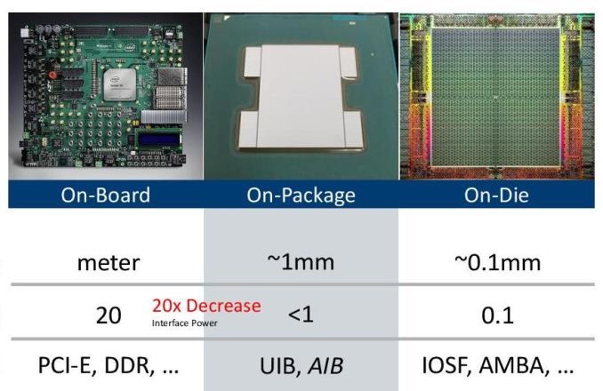
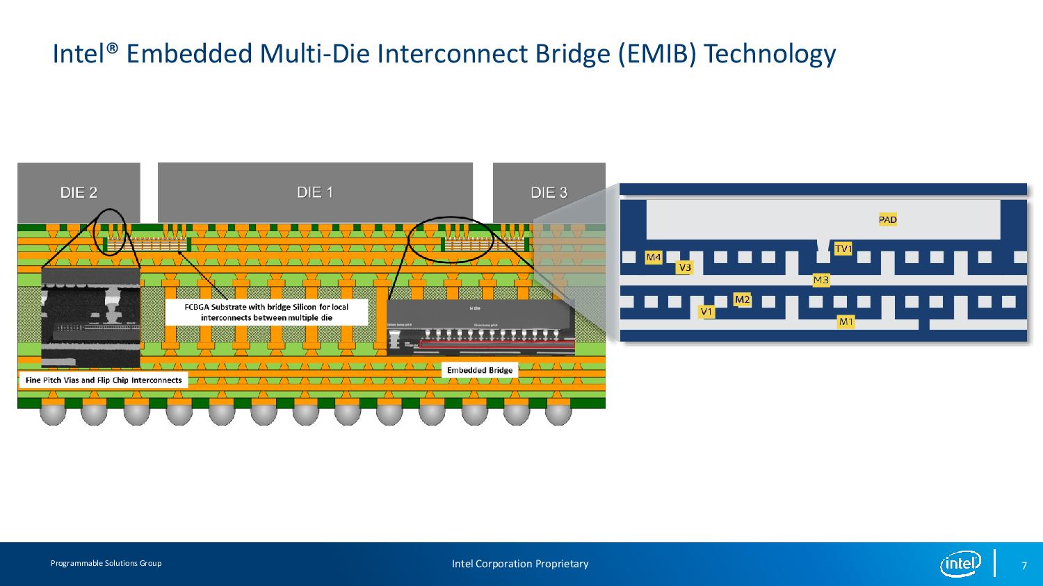
11:28AM EDT - Today at Hot Chips we have a lot of interesting talks going on. First up is a talk on Intel's latest 14nm FPGA solution: Stratix 10 implementing HBM using Intel's latest EMIB (embedded multi-die interconnect bridge) technology that may migrate over to enterprise CPUs over the next few years.
11:30AM EDT - Other talks today include Google's TPU, IBM's z CPU, as well as talks on EPYC, Xeon and Centriq (we've covered these before)
11:30AM EDT - Sorry again today we're fighting the WiFi. With today being the busiest day of the conference, I'm expecting there to be strain on the data. So pictures may come after the talks.
11:33AM EDT - Aside from the Stratix 10 FPGA news, EMIB is particularly exciting
11:34AM EDT - As we move to smaller process nodes, it makes massive monolithic chips harder to create. Yields go down and it gets expensive
11:34AM EDT - The solution to this is to create a multi-die package, using interconnects between the chips. We've seen this for years, and most recently in Xeon Phi and EPYC
11:35AM EDT - So while we've had the frequency wars, we're in the Core wars, to a certain extent the server market is in the midst of the communcation wars: how can data be moved in bulk at low latency
11:35AM EDT - Die to die communication now becomes an area calling out for innocation
11:36AM EDT - Standard chip-to-chip communications can come in two main ways. Either through the package, or via an interposer (such as Fiji, Vega, Volta)
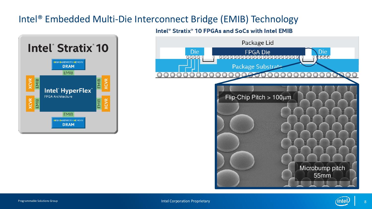
11:36AM EDT - EMIB is a mid-way point in this. Signals still go through the package, but the package is modified to allow for shorter paths and faster connectivity
11:37AM EDT - As shown on the picture at the top, it allows for silicon dies to get super close as well
11:37AM EDT - Intel has announced EMIB before, most noticeably at their manufacturing tech day earlier this year
11:39AM EDT - We'll see it in FPGAs first, that require access to high bandwidth memory (and customers are willing to pay)
11:39AM EDT - Although the future of the technology can mean that we will have multiple dies on package made at different process nodes. The cores at one node, the onboard memory at another node, perhaps integrated accelerators/RF at other nodes etc
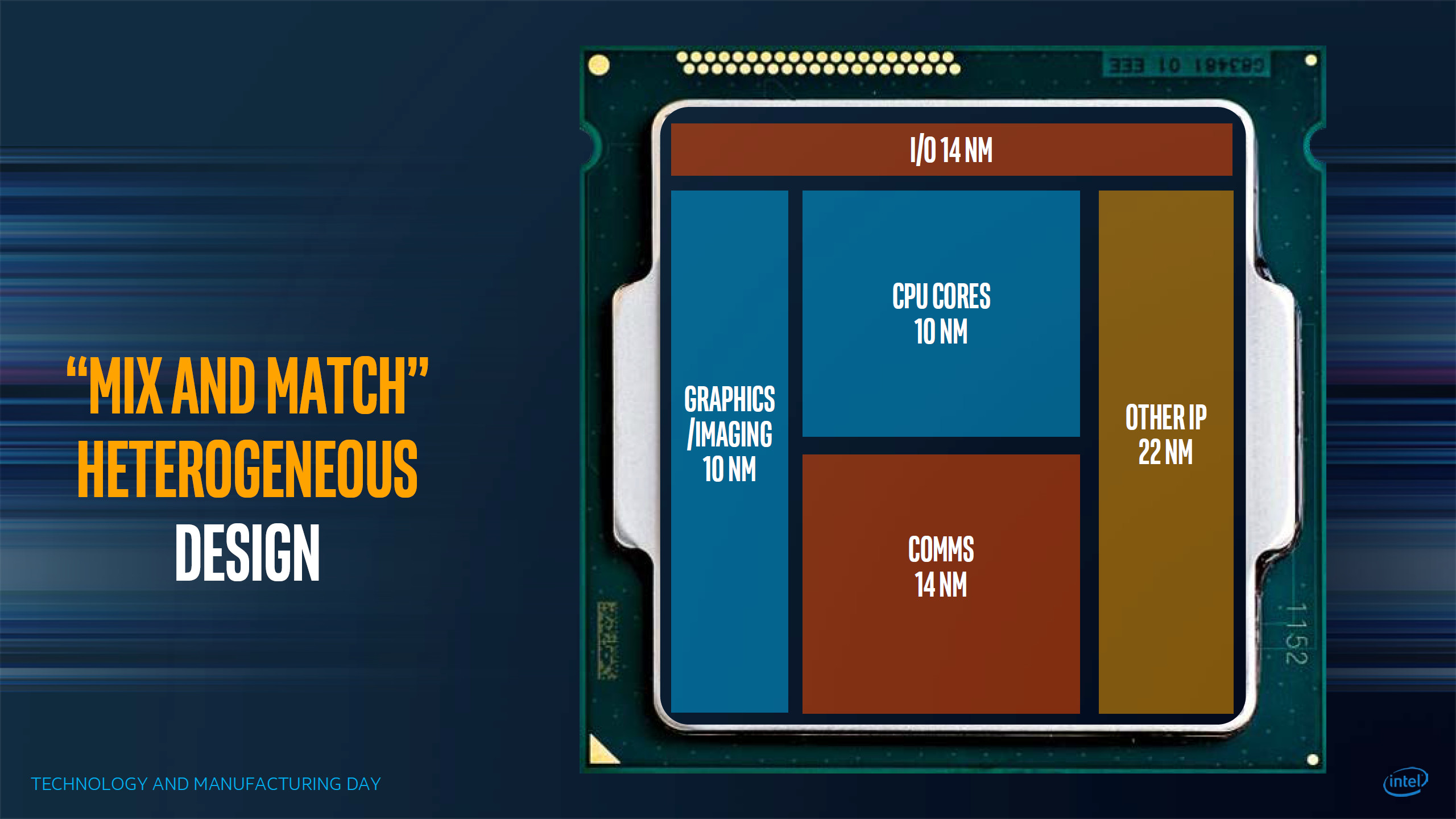
11:41AM EDT - This image is what Intel showed back at the Manufacturing Day
11:41AM EDT - This is why the technology comes across as fascinating to the future of Intel's processor lines. Especially as we hit 10nm and below
11:41AM EDT - Obviously the other semiconductor companies will have to implement their own solution, whether it is through the package or using an interposer
11:42AM EDT - I'll be uploading the slides as quick as I can as the talk progresses. Should start in a few minutes
11:48AM EDT - OK here we go
11:50AM EDT - As time goes on, packaging features are more of the platform over than the silicon
11:50AM EDT - Long dev cycles
11:51AM EDT - So high non-recurring engineering cost and longer time to market
11:51AM EDT - So develop a new packaging technology to help this
11:52AM EDT - 'Amortize the engineering over several identical items, or evolve flexible technologies'
11:52AM EDT - 'Build a large system out of smaller parts.
11:54AM EDT - Small sliver of silicon in the package
11:54AM EDT - Now Build the system: Intel Stratix 10 with four tranceiver chiplets and two DRAM chiplets
11:56AM EDT - Now Build the system: Intel Stratix 10 with four tranceiver chiplets and two DRAM chiplets
11:57AM EDT - Using multibump pitch on the FPGA die
11:57AM EDT - Interposer is also available, but EMIB is only localised digital connections. Other IOs/RG are unaffected, and can use multiple bridges. In an interposer, you need to have TSVs for non-cross chip communication. All the signals need to go through
11:58AM EDT - So reduced fabrication and assembly, cost effective, high perf solution. Also no reticle size limits now: build a system as large as your package.
11:58AM EDT - So comparison: onboard routing is 20 pJ/b (PCIe, DDR), on-die is 0.1 pJ/b (AMBA, IOSF), But with EMIB, distance is 100 micron, power is under 1pJ/b
11:58AM EDT - So defining the standard. Data rate as a function of brakout density (IO per mm at die edge)
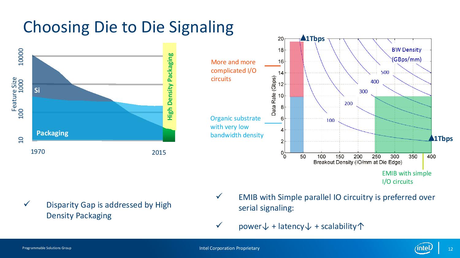
11:59AM EDT - EMIB is a simple parallel IO circuitry for lower power and lower latency and larger scalability
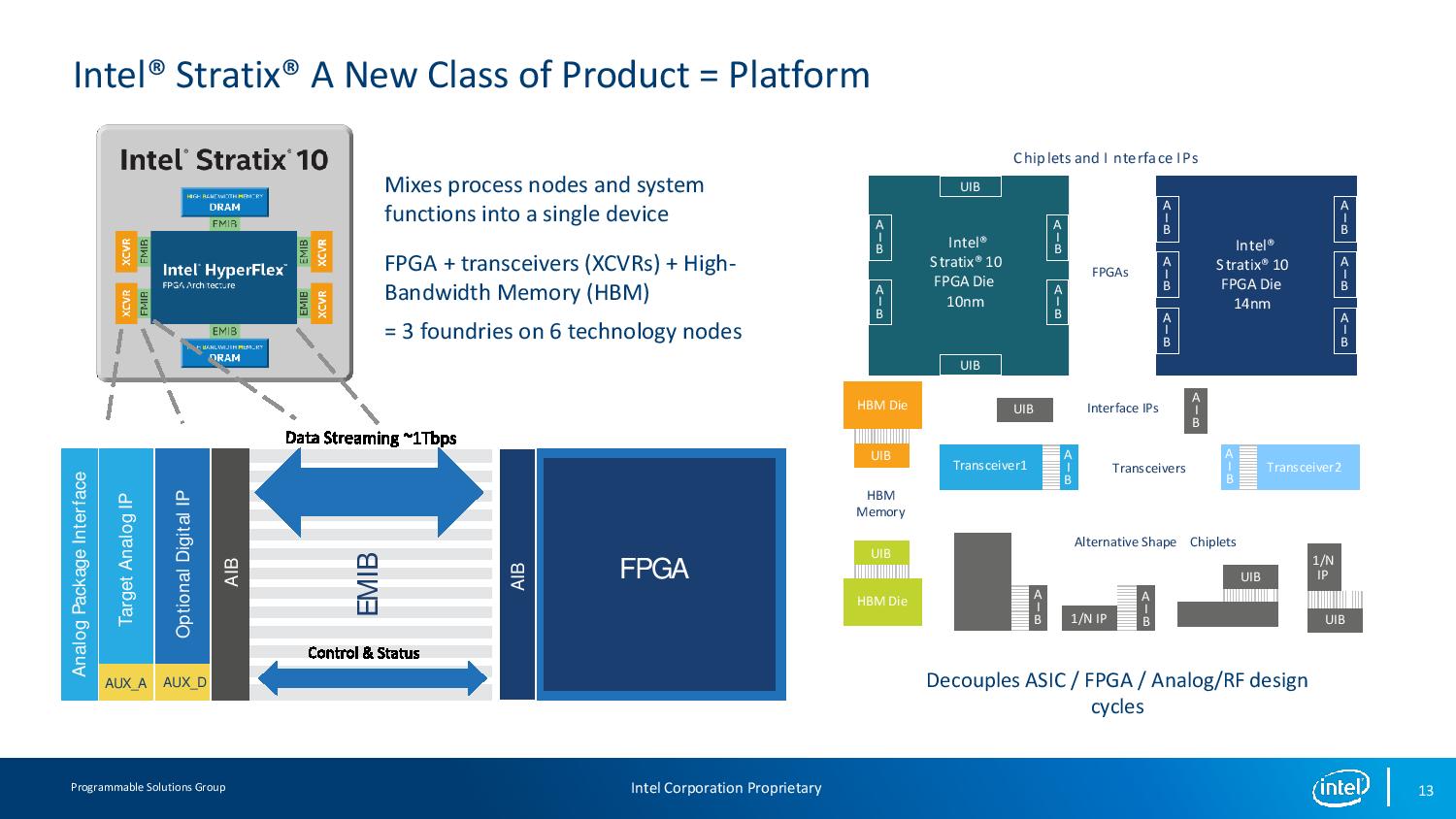
12:01PM EDT - AIB a small sliver for communication and data streaming at 1 Tbps
12:01PM EDT - AIB on chiplet and AIB on FPGA. Now it becomes a Lego system. Stick what you need together when the AIB is standard
12:01PM EDT - Chiplets can be large or small as whatever is needed. Chiplets can have multiple AIBs to connect to other silicon.
12:01PM EDT - Also use multi-foundry and multi-node
12:02PM EDT - for noise isolation, superior for analog vs monolithic
12:02PM EDT - proven on 3 foundries on 6 tech nodes
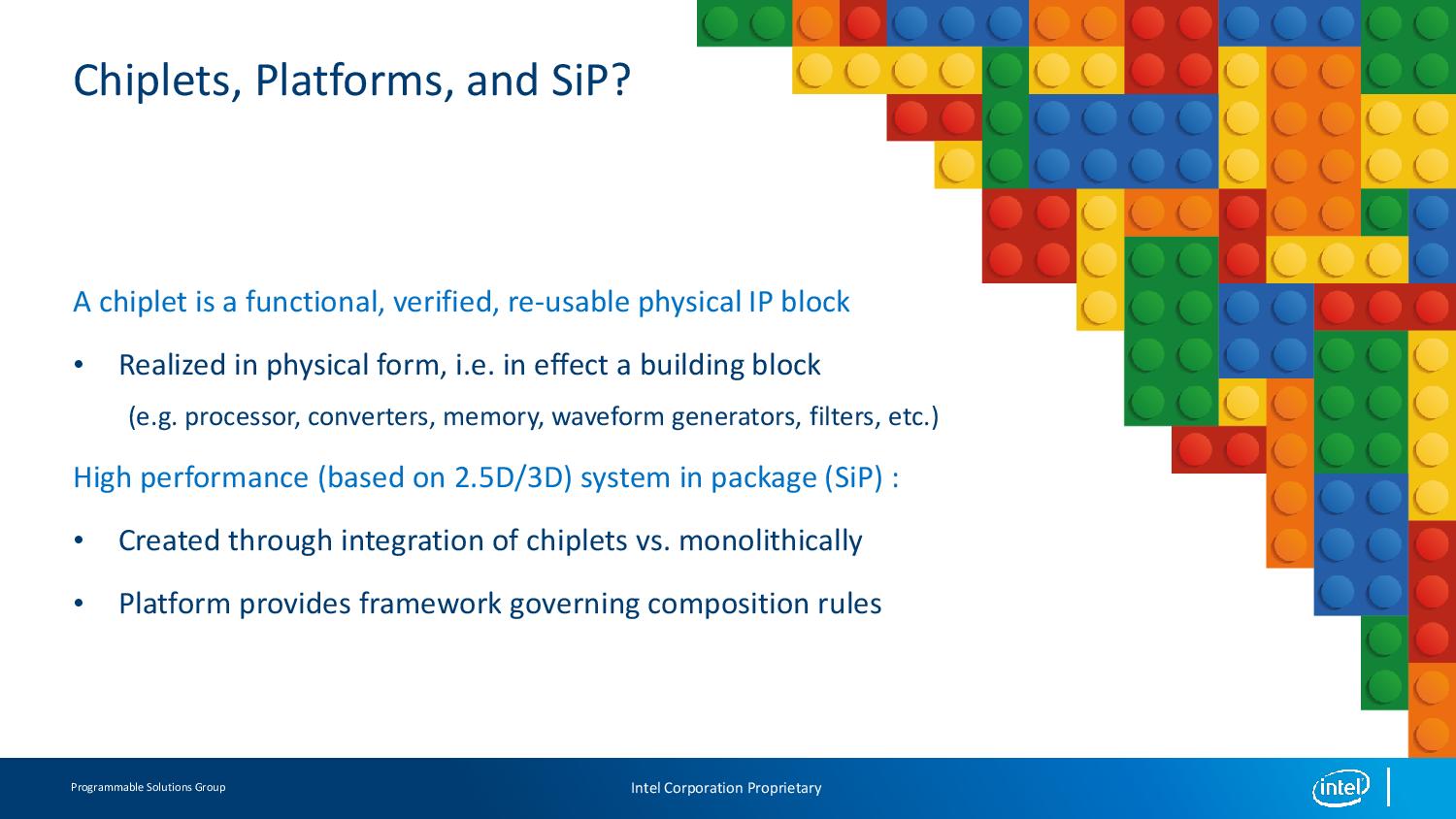
12:03PM EDT - Chiplets are functional IP blocks in a physical form - in effect a building block
12:03PM EDT - Platform needs simple composition rules
12:03PM EDT - So AIB and UIB

12:03PM EDT - Perhaps there are a couple of different classes of applications
12:04PM EDT - UIB is general purpose SiP for HBM/ASIC
12:04PM EDT - AIB for transciever and analog/RF
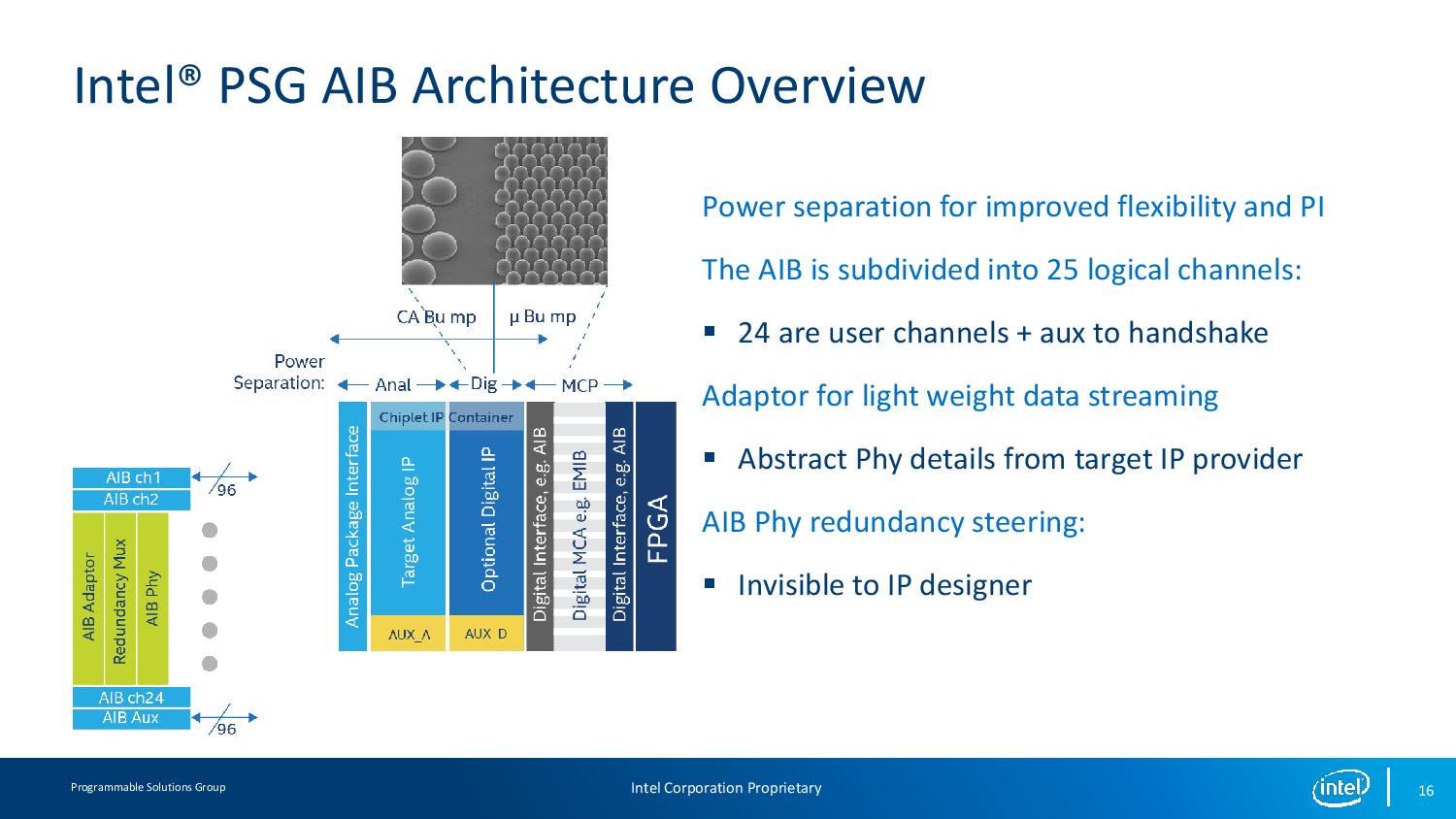
12:05PM EDT - AIB has 25 logical channels - 24 for user, one for handshake
12:05PM EDT - adaptor for light weight data streaming and redundancy steering
12:06PM EDT - IP designer can focus on IP design, rather than connectivity
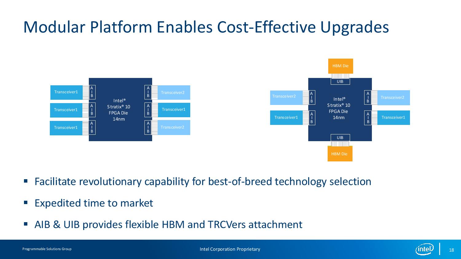
12:07PM EDT - Create dies with AIB and UIB ports, then play lego to create a family of products
12:07PM EDT - Modular platform enables cost-effective upgrades. No need to respin a die, just replace chiplets with other IP blocks
12:07PM EDT - e.g. new generation transceivers or new HBM. Reduces time to market
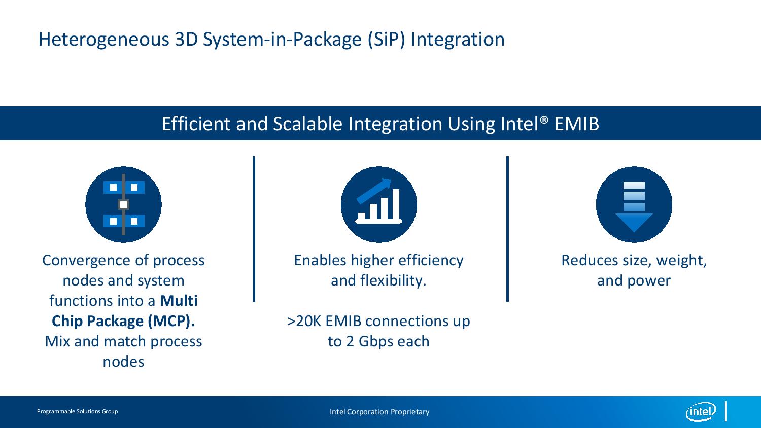
12:09PM EDT - Can now converge both process nodes and suitable cost
12:09PM EDT - 20K EMIB connections up to 2 Gbps each
12:09PM EDT - Reduces size, weight and power

12:10PM EDT - EMIB isn't about a particular product, but rolling out on Stratix first
12:10PM EDT - More use of EMIB through DARPA and 'Chips' (?)
12:11PM EDT - 'No company has a monopoly on innovation - we want to innovate with partners'
12:11PM EDT - Time for Q&A
12:12PM EDT - 'Q: How available is EMIB'
12:14PM EDT - 'A: Cost analysis makes yield of EMIB preferable over other technology. High-end and mid-range systems are coming from Intel using EMIB'
12:14PM EDT - 'Q: are there pitch bump limits'
12:15PM EDT - 'A: we're at 55 now, with 35 coming soon. We've seen as low as 10 micron in the lab'
12:17PM EDT - 'Q: Chiplets idea is good, but interposers are for high volume. Can I go to Intel and use their EMIB technology?'
12:18PM EDT - A: Intel has EMIB, but GloFo had interposer. Three foundries here, should drive the cost down. If the business model is right, Intel would build high-volume EMIB but there is no monopoly on high-density packaging technology
12:18PM EDT - 'Q: Is EMIB ready for prime time?'
12:19PM EDT - 'A: Yes, EMIB is in the field, and large volumes are coming and it is ready for prime time'
12:20PM EDT - 'Q: Can you get around bad dies before putting chiplets onto the package?' 'A: Yes'
12:21PM EDT - 'Q: Can you get around bad dies before putting chiplets onto the package?' 'A: Yes'
12:23PM EDT - 'Q: Can you get around bad dies before putting chiplets onto the package?' 'A: Yes'
12:23PM EDT - That's a wrap. Xilinx are now doing a talk on a new 16nm FPGA with HBM and CCIX


51 Comments
View All Comments
TeaMat - Tuesday, August 22, 2017 - link
Pfft, this is just glued together ;)Lieutenant Tofu - Wednesday, August 23, 2017 - link
Wait, Intel is planning on .. GLUING TOGETHER multiple IP blocks?! ;)Smell This - Wednesday, August 23, 2017 - link
So ...I don't want to incorrectly label or falsely characterize this, but Intel "Stratix" is the continuation/integration or 2017 modernization of Altera IP (which they acquired in 2015) ... as a response to Advanced Micro Device's decade-long quest for '3D-IC' and bolt-on fusion of disparate technologies ??
If this is correct, I guess imitation (in efforts to exert market heft) is truly the greatest form of flattery ...
patrickjp93 - Friday, August 25, 2017 - link
Except Intel has completely overhauled Altera's designs. There's practically nothing in common with the old designs. Block and cell-level programming, not to mention transform times and overall performance/watt have gone from incredible to a scale Xilinx is in no position to compete with.kfishy - Saturday, August 26, 2017 - link
Stratix 10 was developed long before the Intel acquisition. Intel FPGA is essentially still clearing the pipes of old Altera designs.patrickjp93 - Monday, September 4, 2017 - link
Hah! No. Altera never had integration this broad, and as for the raw design of the FPGA itself, it's in a completely different league than before thanks to Intel's design libraries. The caching structure is completely different too.No, it may not be a 100% Intel design, but it is very far removed from Altera already.
Ian Cutress - Friday, August 25, 2017 - link
Android Password Breaker hacking tutorials hacking ebooks hacking news hacking tools android technology https://myhacker.netSaolDan - Friday, August 25, 2017 - link
did u just get hacked?Santoval - Saturday, August 26, 2017 - link
So Intel will move to "glued" dies, just as AMD, but -in their analogy- due to EMIB they will instead use... super-glue?Santoval - Saturday, August 26, 2017 - link
p.s. Unless I missed something and they intend to use "super-glued" dies only for their FPGAs. But I don't think they developed EMIB solely for them, did they?