Hot Chips 2016: NVIDIA Discloses Tegra Parker Details
by Joshua Ho on August 25, 2016 11:00 AM EST- Posted in
- Mobile
- Hot Chips
- Project Denver
- Trade Shows
- NVIDIA
- Tegra
- Tegra Parker
At CES 2016 we saw that DRIVE PX2 had a new Tegra SoC in it, but to some extent NVIDIA was still being fairly cagey about what was actually in this SoC or what the block diagram for any of these platforms really looked like. Fortunately, at Hot Chips 2016 we finally got to see some details around the architecture of both Tegra Parker and DRIVE PX2.
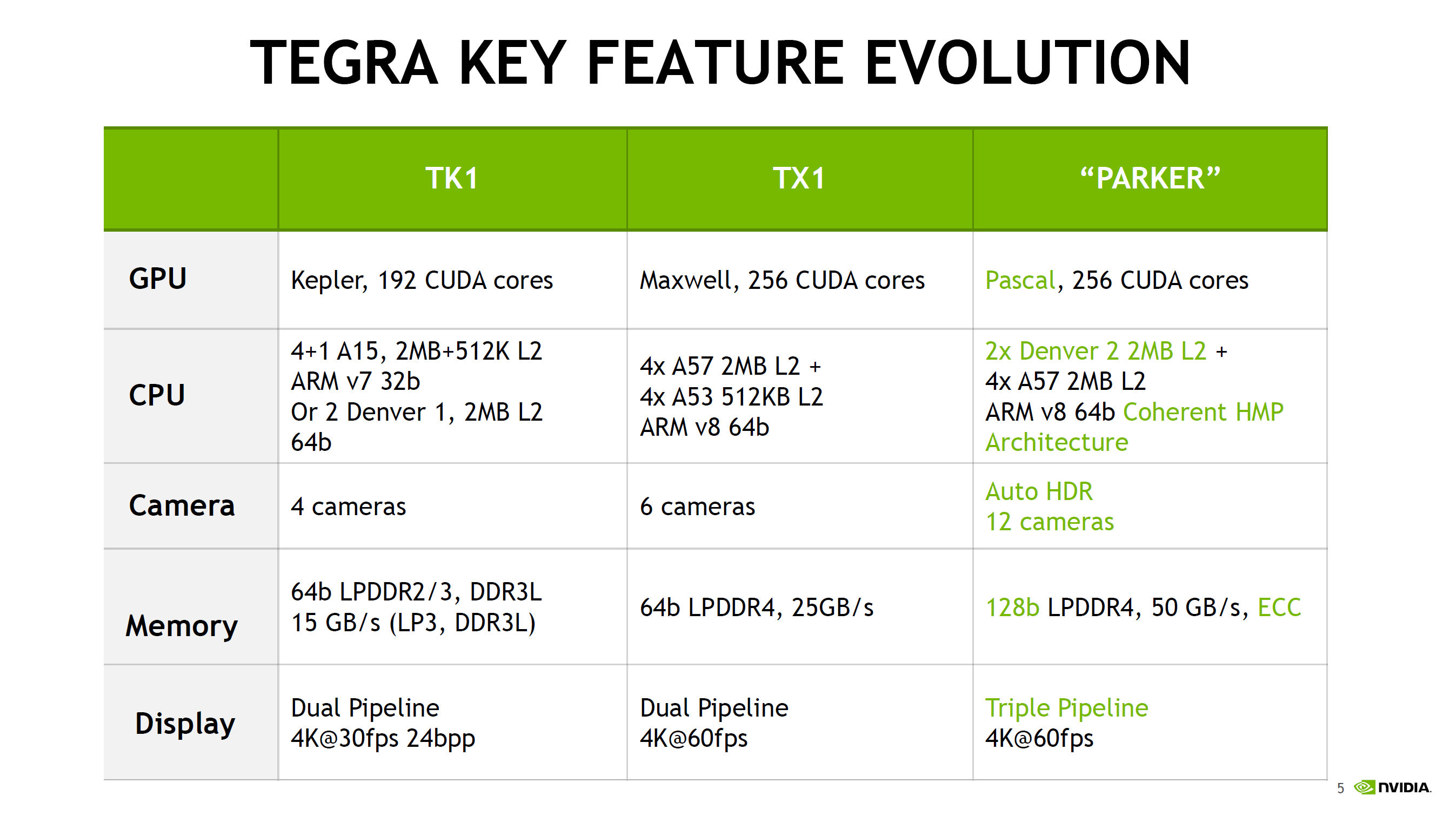
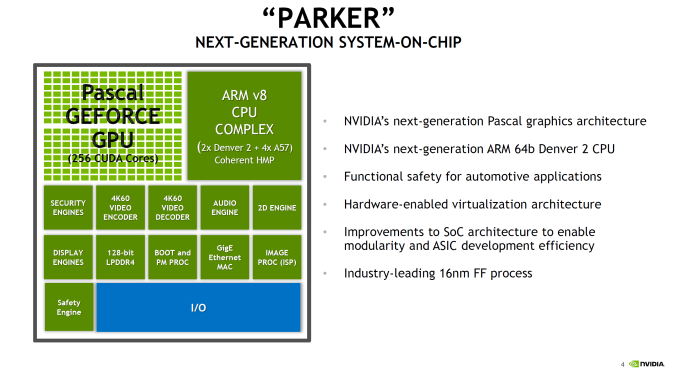
Starting with Parker, this is an SoC that has been a long time coming for NVIDIA. The codename and its basic architectural composition were announced all the way back at GTC in 2013, as the successor to the Logan (Tegra K1) SoC. However Erista (Tegra X1) was later added mid-generation - and wound up being NVIDIA's 20nm generation SoC - so until now the fate of Parker has not been clear. As it turns out, Parker is largely in line with NVIDIA's original 2013 announcement, except instead of a Maxwell GPU we get something based off of the newer Pascal architecture.
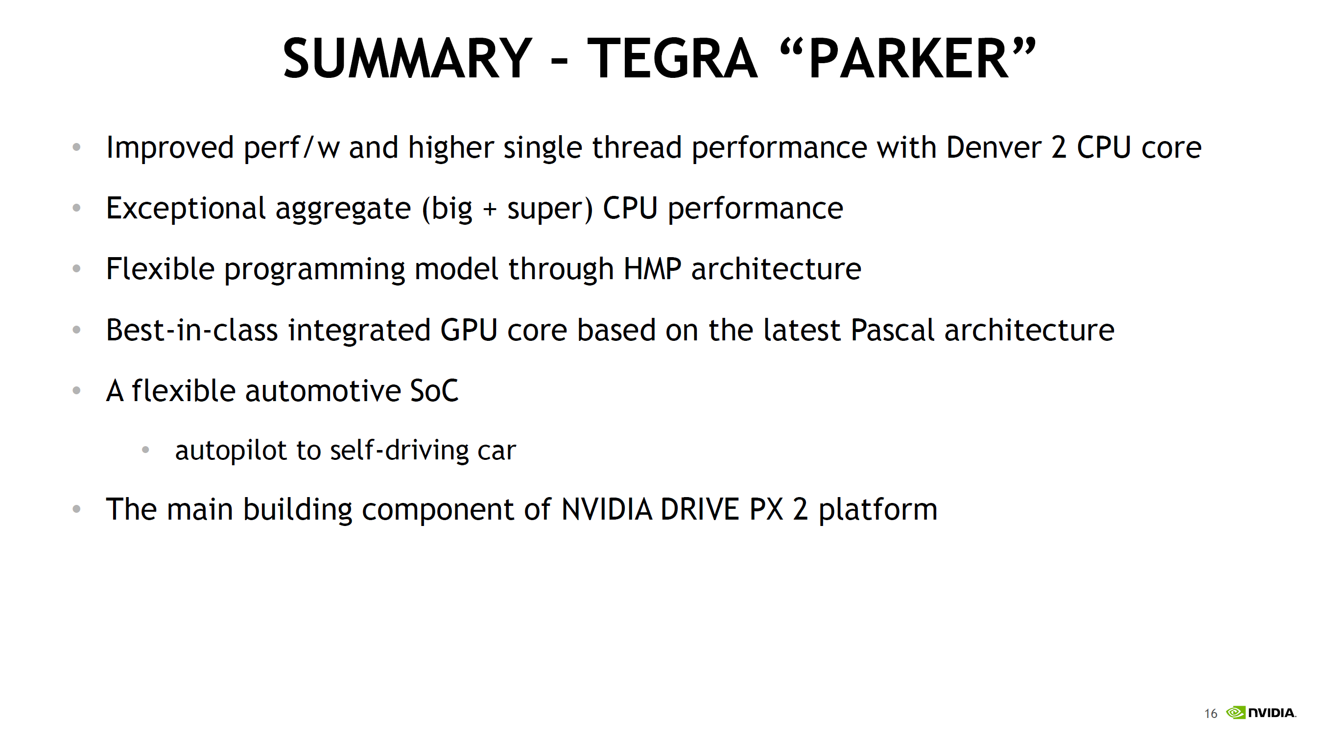
But first, let's talk about the CPU. The CPU complex has been disclosed as a dual core Denver 2 combined with a quad core Cortex A57, with the entire SoC running on TSMC 16nm FinFET process. This marks the second SoC to use NVIDIA's custom-developed ARM CPU core, the first being the Denver version of the Tegra K1. Relative to K1, Parker (I suspect NVIDIA doesn't want to end up with TP1 here) represents both an upgrade to the Denver CPU core itself, and how NVIDIA structures their overall CPU complex, with the addition of a quartet of ARM Cortex-A57 cores joining the two Denver 2 cores.
The big question for most readers, I suspect, is about the Denver 2 CPU cores. NVIDIA hasn't said a whole lot about them - bearing in mind that Hot Chips is not an exhaustive deep-dive style architecture event - so unfortunately there's not a ton of information to work with. What NVIDIA has said is that they've worked to improve the overall power efficiency of the cores (though I'm not sure if this factors in 16nm FinFET or not), including by implementing some new low power states. Meanwhile on the performance side of matters, NVIDIA has confirmed that this is still a 7-wide design, and that Denver 2 uses "an improved dynamic code optimization algorithm." What little that was said about Denver 2 in particular was focused on energy efficiency, so it may very well be that the execution architecture is not substantially different from Denver 1's.
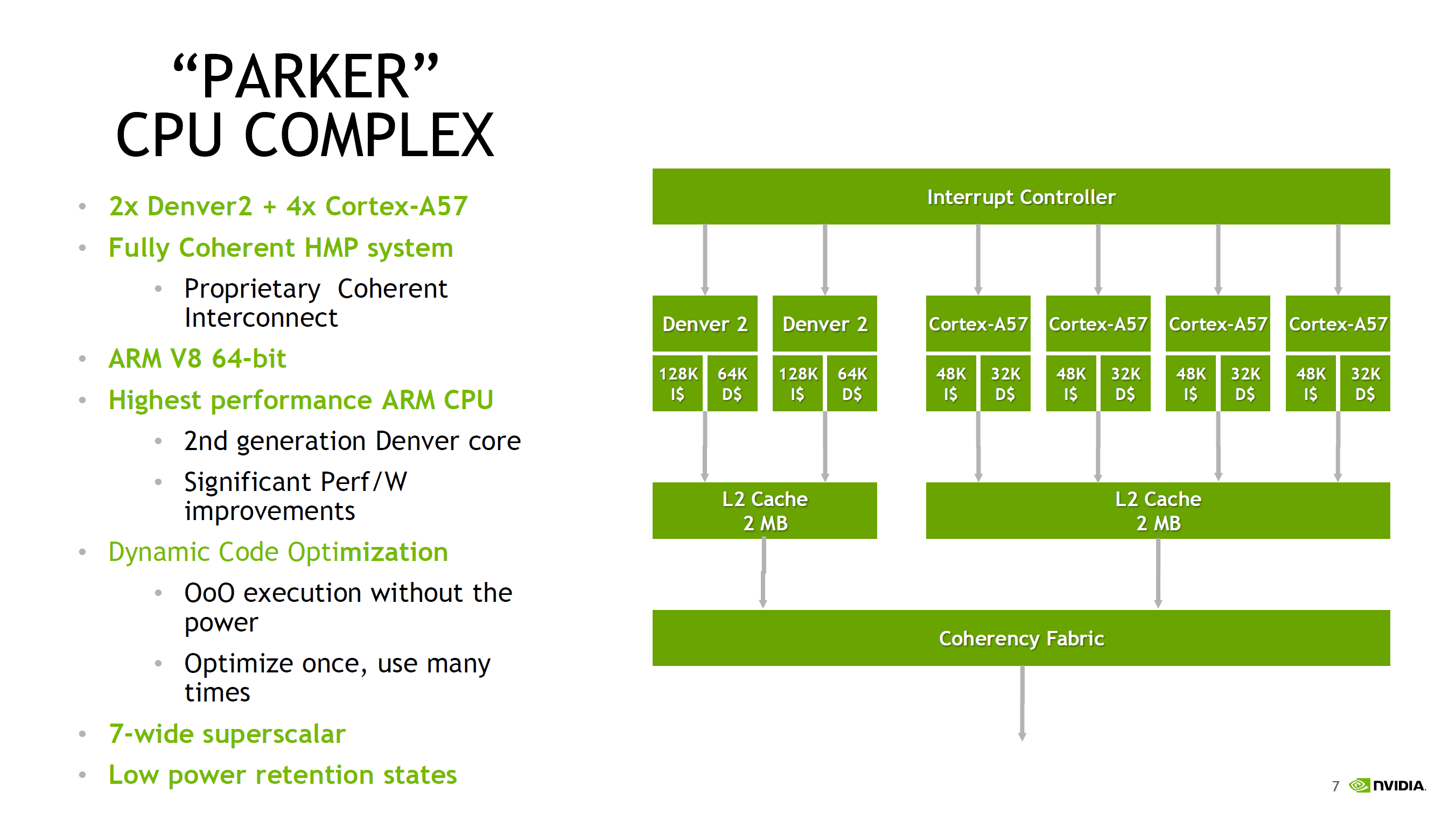
With that in mind, the bigger news from a performance standpoint is that with Parker, the Denver CPU cores are not alone. For Parker the CPU has evolved into a full CPU complex, pairing up the two Denver cores with a quad-core Cortex-A57 implementation. NVIDIA cheekily refers to this as "Big + Super", a subversion of ARM's big.LITTLE design, as this combines "big" A57 cores with the "super" Denver cores. There are no formal low power cores here, so when it comes to low power operation it looks like NVIDIA is relying on Denver.
That NVIDIA would pair up Denver with ARM's cores is an interesting move, in part because Denver was originally meant to solve the middling single-threaded performance of ARM's earlier A-series cores. Secondary to this was avoiding big.LITTLE-style computing by making a core that could scale the full range. For Parker this is still the case, but NVIDIA seems to have come to the conclusion that both responsiveness and the total performance of the CPU complex needed addressed. The end result is the quad-core A57 to join the two Denver cores.
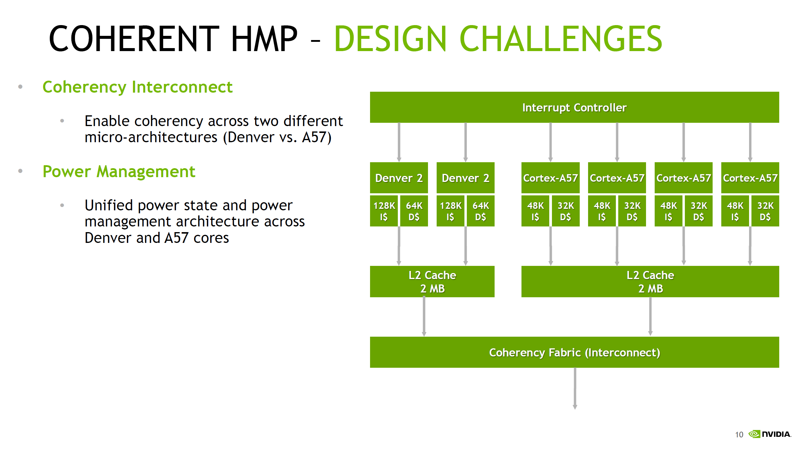
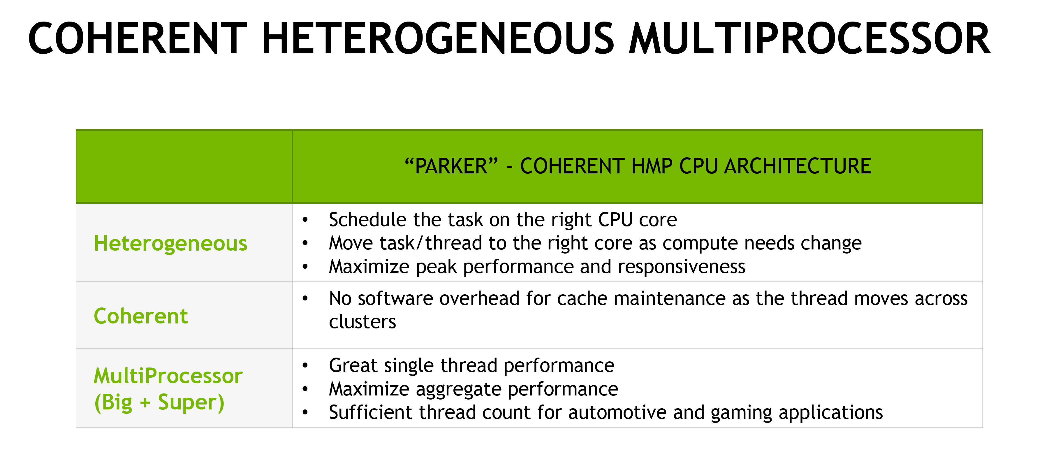
NVIDIA didn't just stop at adding A57 cores though; they also made the design a full Heterogeneous Multi-Processing (HMP) design. A fully coherent HMP design at that, utilizing a proprietary coherency fabric specifically to allow the two rather different CPU cores to maintain that coherency. The significance of this - besides the unusual CPU pairing - is that it should allow NVIDIA to efficiently migrate threads between the Denver and A57 cores as power and performance require it. This also allows NVIDIA to use all 6 CPU cores at once to maximize performance. And since Parker is primarily meant for automotive applications - featuring more power and better cooling - unlike mobile environments it's entirely reasonable to expect that the design can sustain operation across all 6 of those CPU cores for extended periods of time.
Overall this setup is very close to big.LITTLE, except with the Denver cores seemingly encompassing parts of both "big" and "little" depending on the task. With all of that said however, it should be noted that NVIDIA has not had great luck with multiple CPU clusters; Tegra X1 featured cluster migration, but it never seemed to use its A53 CPU cores at all. So without having had a chance to see Parker's HMP in action, I have some skepticism on how well HMP is working in Parker.
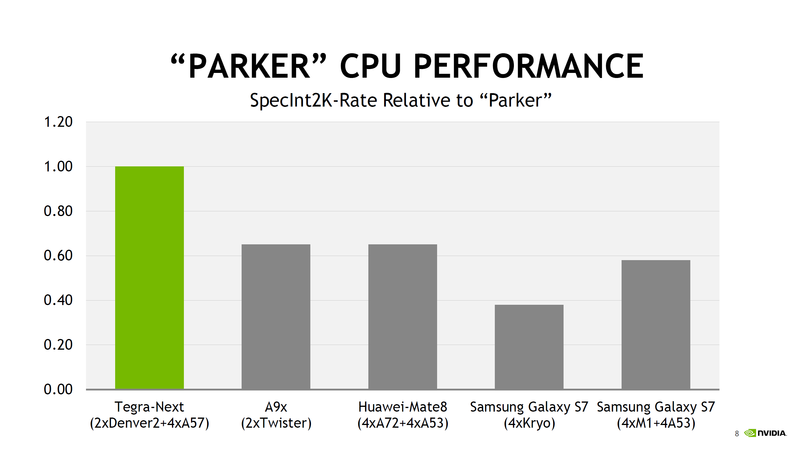
Overall, NVIDIA is claiming about 40-50% more overall CPU performance than A9x or Kirin 950, which is to say that if your workload can take advantage of all 6 CPUs in the system then it’s going to be noticeably faster than two Twister CPUs at 2.2 GHz. But there’s no comparison to Denver 1 (TK1) here, or any discussion of single-thread performance. Though on the latter, admittedly I'm not sure quite how relevant that is for NVIDIA now that Parker is primarily an automotive SoC rather than a general purpose SoC.

Outside of the CPU, NVIDIA has added some new features to Parker such as doubling memory bandwidth. For the longest time NVIDIA stuck with a 64-bit memory bus on what was essentially a tablet SoC lineup, which despite what you may think from the specs worked well enough for NVIDIA, presumably due to their experience in GPU designs, and as we've since learned, compression & tiling. Parker in turn finally moves to a 128-bit memory bus, doubling the aggregate memory bandwidth to 50GB/sec (which works out to roughly LPDDR4-3200).
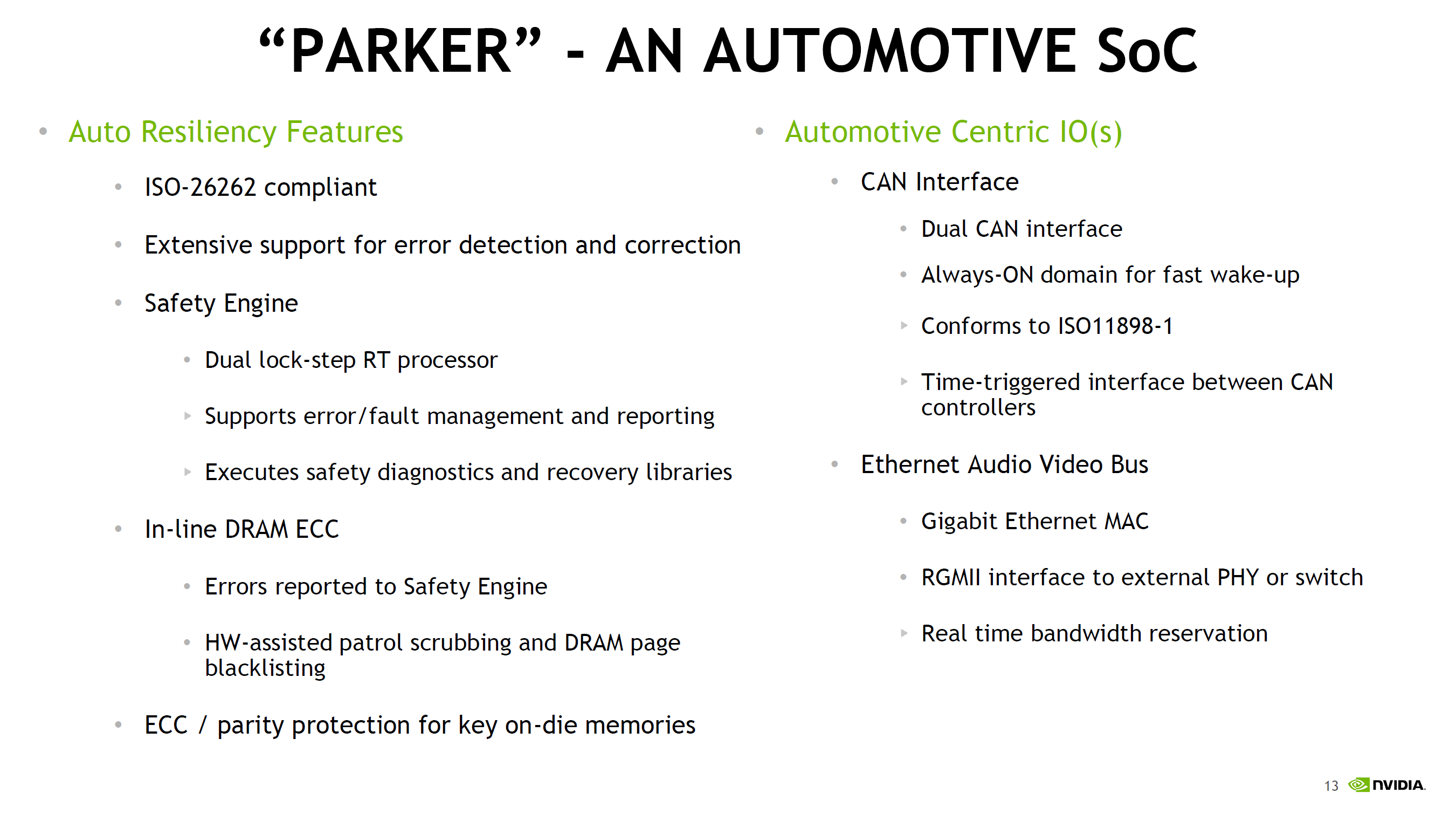
More interesting however is the addition of ECC support to the memory subsystem. This seems to be in place specfically to address the automotive market by improving the reliability of the memory and SoC. A cell phone and its user can deal with the rare bitflip, however things like self-driving vehicles can't afford the same luxury. Though I should note it's not clear whether ECC support is just some kind of soft ECC for the memory or if it's hardwired ECC (NVIDIA calls it "in-line" DRAM ECC). But it's clear that whatever it is, it extends beyond the DRAM, as NVIDIA notes that there's ECC or parity protection for "key on-die memories", which is something we'd expect to see on a more hardened design like NVIDIA is promoting.
Finally, NVIDIA has also significantly improved their I/O functionality, which again is being promoted particularly with the context of automotive applications. There’s more support for extra cameras to improve ADAS and self-driving systems, as well as 4Kp60 video encode, CAN bus support, hardware virtualization, and additional safety features that help to make this SoC truly automotive-focused.
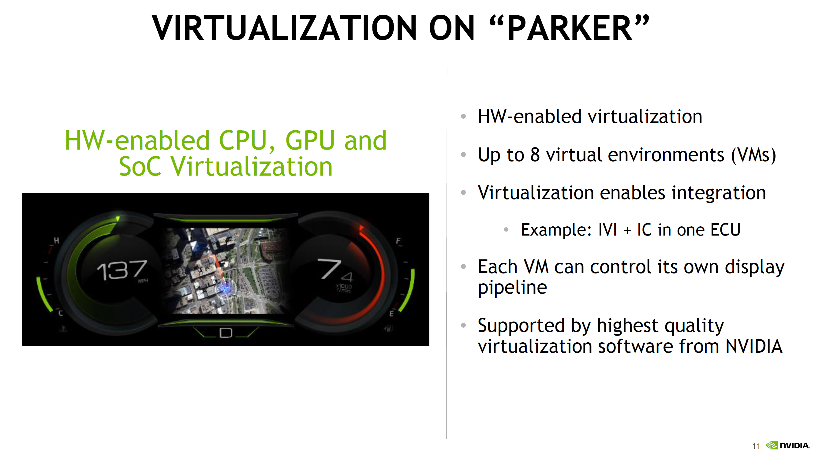

The hardware virtualization of Parker is particularly interesting. It's both a safety feature - isolating various systems from each other - while also allowing for some cost reduction on the part of the OEM as there is less need to use separate hardware to avoid a single point of failure for critical systems. There’s a lot of extra logic going on to make this all work properly, and things like running the dual Parker SoCs in a soft lockstep mode is also possible. In the case of DRIVE PX2 an Aurix TC297 is used to function as a safety system and controls both of the Parker SoCs, with a PCI-E switch to connect the SoCs to the GPUs and to each other.
Meanwhile, it's interesting to note that the GPU of Parker was not a big part of NVIDIA's presentation. Part of this is because Parker's GPU architecture, Pascal, has already launched in desktops and is essentially a known quantity now. At the same time, Parker's big use (at least within NVIDIA) is for the DRIVE PX2 system, which is going to be combining Parker with a pair of dGPUs. So in the big picture Parker's greater role is in its CPUs, I/O, and system management rather than its iGPU.
Either way, NVIDIA's presentation confirms that Parker integrates a 256 CUDA Core Pascal design. This is the same number of CUDA Cores as on TX1, so there has not been a gross increase in GPU hardware. At the same time moving from TSMC's 20nm planar process to their 16nm FinFET process did not significantly increase transistor density, so there's also not a lot of new space to put GPU hardware. NVIDIA quotes an FP16 rate of 1.5 TFLOPs for Parker, which implies a GPU clockspeed of around 1.5GHz. This is consistent with other Pascal-based GPUs in that NVIDIA seems to have invested most of their 16nm gains into ramping up clockspeeds rather than making for wider GPUs.
As the unique Maxwell implementation in TX1 was already closer to Pascal than any NVIDIA dGPU - in particular, it supported double rate FP16 when no other Maxwell did - the change from Maxwell to Pascal isn't as dramatic here. However some of Pascal's other changes, such as fine-grained context switching for CUDA applications, seems to play into Parker's other features such as hardware virtualization. So Pascal should still be a notable improvement over Maxwell for the purposes of Parker.
Overall, it’s interesting to see how Tegra has evolved from being almost purely a mobile-focused SoC to a truly automotive-focused SoC. It’s fairly obvious at this point that Tegra is headed towards higher TDPs than what we’ve seen before, even higher than small tablets. Due to this automotive focus it’ll be interesting to see whether NVIDIA starts to integrate advanced DSPs or anything similar or if they continue to mostly rely on CPU and GPU for most processing tasks.


29 Comments
View All Comments
testbug00 - Friday, August 26, 2016 - link
Automotive is in large part detecting cars around you. For self driving. The last thing I would want is a core which is unpredictible to be handing ANY information of that sort.fanofanand - Thursday, August 25, 2016 - link
A little disappointing to see EMMC being utilized. This is such a mish-mash, high speed DDR4 with ECC next to an A57. Pascal next to EMMC. The validation for automotive must be the reason for such an odd assembly, but I really would hope they would put something together that is far more current for any future tablet/consoles. Denver + A72 with DDR4, Volta, and UFS would be sweet.psychobriggsy - Friday, August 26, 2016 - link
To be fair, it does have SATA as well, and likely some spare PCIe lanes that could be used for an SSD if that's desirable.jwcalla - Thursday, August 25, 2016 - link
"At the same time, Parker's big use (at least within NVIDIA)..."Mmmm hmmm...
Joshua knows something.
HigherState - Friday, August 26, 2016 - link
AVB over ethernet sounds very interesting. I could see the use of a set of rear/side cameras, and maybe the rear speakers connected to a AD/DA hub in the trunk. A single ethernet cable gets run from the hub to the the front of the vehicle (maybe two for redundancy). Should cut down on complexity and weight of all the wires in a harness. Its low latency and already technology that exists today.Jumangi - Friday, August 26, 2016 - link
Great job Nvidia comparing a SoC that goes in a car vs a tiny smartphone case. Totally not Apples to Oranges.daku123 - Friday, August 26, 2016 - link
>> NVIDIA quotes an FP16 rate of 1.5 TFLOPs for Parker, which implies a GPU clockspeed of around 1.5GHz.TFLOPs depends largely on number of cores and how the SOC is designed. Statement above is not particularly geeks friendly :)
tipoo - Friday, August 26, 2016 - link
But we know the architecture and the core count...It's a perfectly reasonable statement.Shaders * 2 floating point operations per cycle * billion cycles per second = theoretical Gflops.
It does not denote performance, it's exactly what it says, theoretical peak Gflops.
darkich - Friday, August 26, 2016 - link
Nintendo NX