SK Hynix Adds HBM2 to Catalog: 4 GB Stacks Set to Be Available in Q3
by Anton Shilov on August 1, 2016 10:00 AM EST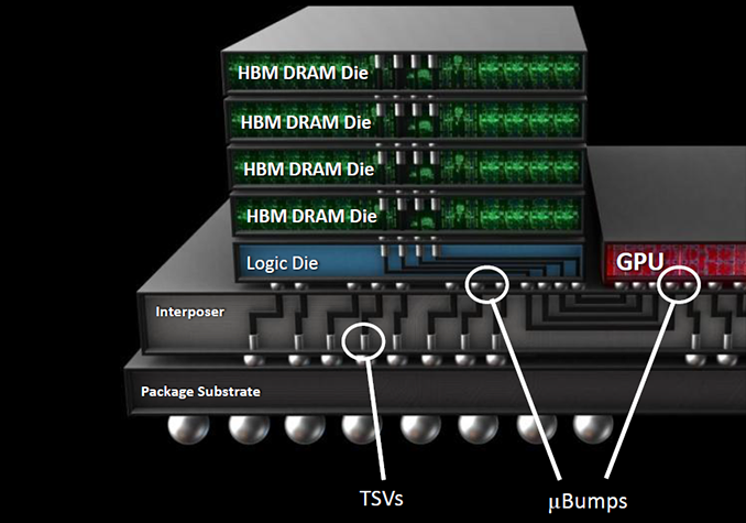
SK Hynix has quietly added its HBM Gen 2 memory stacks to its public product catalog earlier this month, which means that the start of mass production should be imminent. The company will first offer two types of new memory modules with the same capacity, but different transfer-rates, targeting graphics cards, HPC accelerators and other applications. Over time, the HBM2 family will get broader.
SK Hynix intends to initially offer its clients 4 GB HBM2 4Hi stack KGSDs (known good stack dies) based on 8 Gb DRAM devices. The memory devices will feature a 1024-bit bus as well as 1.6 GT/s (H5VR32ESM4H-12C) and 2.0 GT/s (H5VR32ESM4H-20C) data-rates, thus offering 204 GB/s and 256 GB/s peak bandwidth per stack. Earlier this year a representative for SK Hynix revealed plans (in an interview with Golem.de) to start volume production of 4 GB HBM2 KGSDs in Q3 and the addition of the devices into product catalog confirms this information. Keep in mind that memory companies usually make announcements about the start of mass production when they are ready to deliver the first batch of new DRAM to a customer(s). Therefore, it is possible that SK Hynix may already be producing HBM2 stacks.
| Specifications of SK Hynix's HBM2 Memory Chips | ||||||||
| Part Number | Density | Data Rate | Bandwidth per Stack |
Packaging | Feature | Availability | ||
| H5VR32ESM4H-20C | 4 GB | 2.0 GT/s | 256 GB/s | 5mKGSD | 4Hi stack, VDD/VDDQ=1.2V | Q3'16 | ||
| H5VR32ESM4H-12C | 1.6 GT/s | 204 GB/s | ||||||
As outlined in our article published earlier this year, HBM2 memory can stack two, four or eight DRAM devices (2Hi, 4Hi, 8Hi stacks) interconnected using through silicon vias (TSVs) on a base logic die per KGSD (known good stacked die). Each DRAM device features two 128-bit channels, which use DDR signaling with a 2n prefetch architecture (256 bits per memory read and write access) and can operate at their own frequency or even in their own mode. SK Hynix uses 21 nm process technology to make its HBM2 memory and eventually plans to offer 2 GB and 8 GB KGSDs (featuring two or eight 8 Gb DRAM ICs) in addition to 4 GB stacks, aimed at providing memory for various applications. All HBM2 memory products from the company will have 1.2 V VDD/VDDQ and will come in new packages featuring 7.75 mm × 11.87 mm (91.99 mm2) dimensions.
Samsung Electronics began to mass produce its 4 GB 4Hi stack HBM2 KGSDs featuring 2 GT/s data-rate earlier this year and NVIDIA employed the new chips for its GP100 GPU. The first NVIDIA-branded card to use the HBM2 is the Tesla P100 compute accelerator, which has 16 GB of HBM2 memory with 720 GB/s bandwidth (as the DRAM interface operates at about 1.4 GT/s data-rate).

Speaking of HBM2 usage by commercial SoCs, last year SK Hynix said that it worked with 10 companies on various projects (including ASICs, x86 processors, ASSPs and FPGAs) featuring HBM memory (both generations), which indicates that the interest for multi-layer high-bandwidth DRAM is here. However, so far only AMD and NVIDIA have introduced actual products featuring HBM and HBM2.
When it comes to the original HBM, it is worth to mention that SK Hynix has removed such stacks from its catalog. It is unknown whether the company continues to ship them to interested parties, but given the fact that there are not a lot of products that utilize HBM1 today, small scale shipments should not be a problem (at least, until SK Hynix phases out its 29 nm production lines). Meanwhile, since HBM2 is here, it is feasible to assume that we are not going to see many new devices utilizing HBM1.
Source: SK Hynix


43 Comments
View All Comments
Alexvrb - Monday, August 1, 2016 - link
Not a big fan of KB himself but Brent Justice's review of the 1060 on [H] was pretty decent. It was even-handed not only in terms of numbers but the language of the review and the conclusion.Roland00Address - Tuesday, August 2, 2016 - link
>Did I mention the all-new and shiny RX-480 gets beaten by 2013's 3.5GB GTX 970Anandtech has the gtx 970 launch being september 2014
http://www.anandtech.com/show/8526/nvidia-geforce-...
Thus your point about the gtx970s and their launch date is very much hyperbole
Flunk - Monday, August 1, 2016 - link
There are a lot of nutcases out there.ImSpartacus - Monday, August 1, 2016 - link
Yeah, big Vega could take three of those 1.6GT/s stacks and yield the same capacity with 25ish% more bandwidth than the Titan X.And then little Vega could use two stacks, but that would have 25ish% more bandwidth than the 1080.
I'm wondering if amd will underclock it a little bit. They generally need more bandwidth than Nvidia, but not THAT much more.
extide - Monday, August 1, 2016 - link
Little Vega: 2x 4GB statcks, 8GB, 2048-bit, 408-512GB/secBig Vega: 4x 4GB stacks, 16GB, 4096-bit, 816-1024GB/sec
Seems like you could build a nice little GPU with 2 of those stacks...
ImSpartacus - Monday, August 1, 2016 - link
Yeah, I think that's why little Vega exists. It's definitely looking like it'll have two stacks and compete with gp104.And looking at bandwidth, it appears like amd could use the 160 MHz variants and still have buckets of bandwidth to spare.
Regarding big Vega, do you think big Vega will be twice (or nearly twice) as large as little Vega?
I would've assumed that big Vega would be more like 1.5x little Vega (just like gp102 is 1.5x gp104), but that would require 3 stacks of hbm and that doesn't appear to be a possible configuration. That's a shame as it would be pretty much perfect (same capacity as non-clamshell 8Gb gp102), but still copious amounts of bandwidth.
RaichuPls - Monday, August 1, 2016 - link
1060 review? RX480 deep dive?gijames1225 - Monday, August 1, 2016 - link
Hopefully this paves the way to upper-end AMD Zen APUs having some HBM on-die for the graphics side of things.haukionkannel - Monday, August 1, 2016 - link
The really interesting thing is how much these memories cost compared to gddr5 and gddr5+. If it is substantially more expensive, as one could ques, then the end product is not very affordable either.But good to know that memory is in schedule, and that means that we can see products based on it in the next year.
stardude82 - Monday, August 1, 2016 - link
I think you mean on-package rather than on-die. Intel Iris Pro graphics and eDRAM operate off-die on-package.